

Driver circuit
a driver circuit and circuit technology, applied in logic circuits, oscillator generators, pulse techniques, etc., can solve problems such as eye waveforms that may not meet specifications, and achieve the effect of reducing the temperature variation in the output signal amplitude of the driver circui
- Summary
- Abstract
- Description
- Claims
- Application Information
AI Technical Summary
Benefits of technology
Problems solved by technology
Method used
Image

Examples
first embodiment
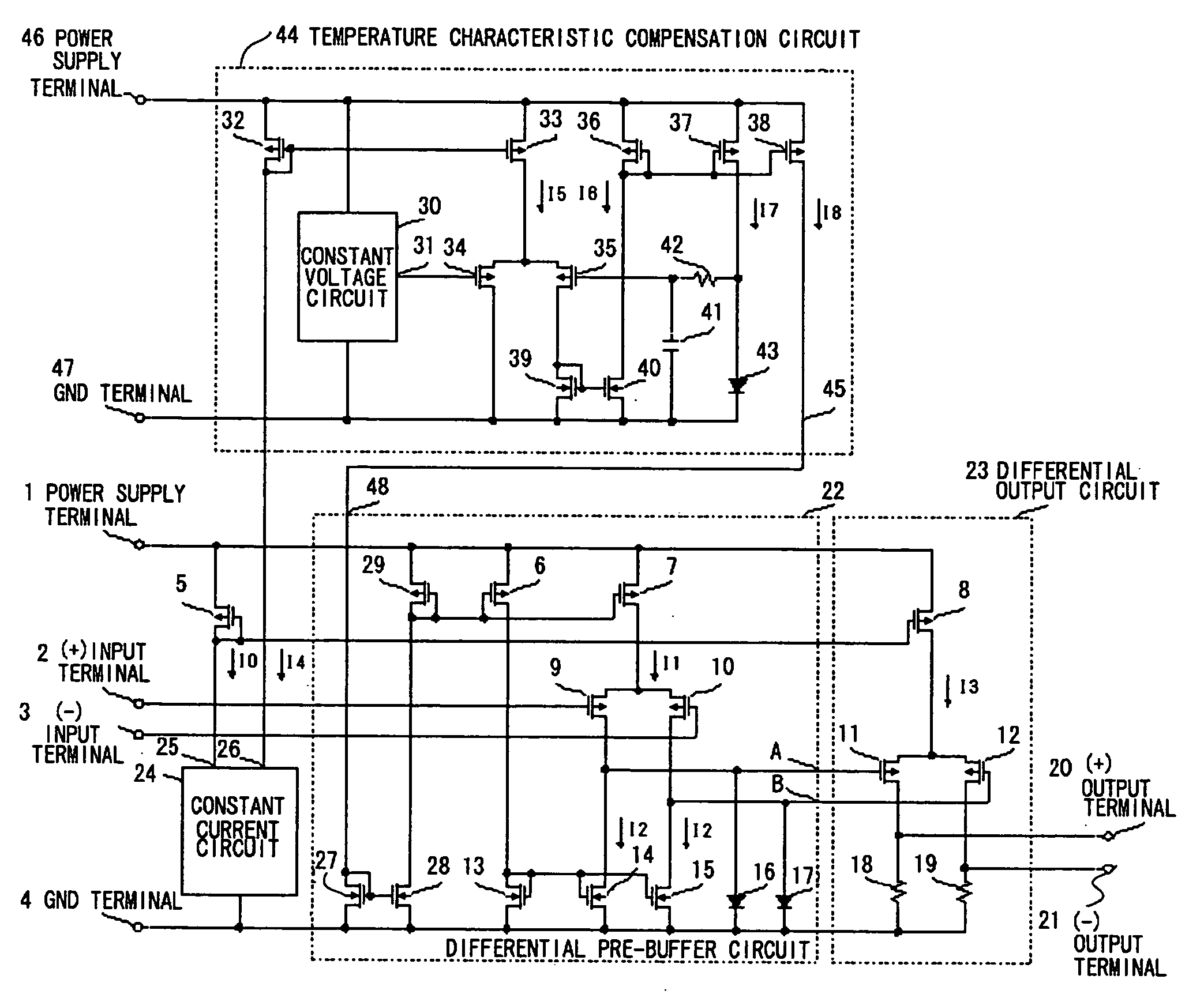
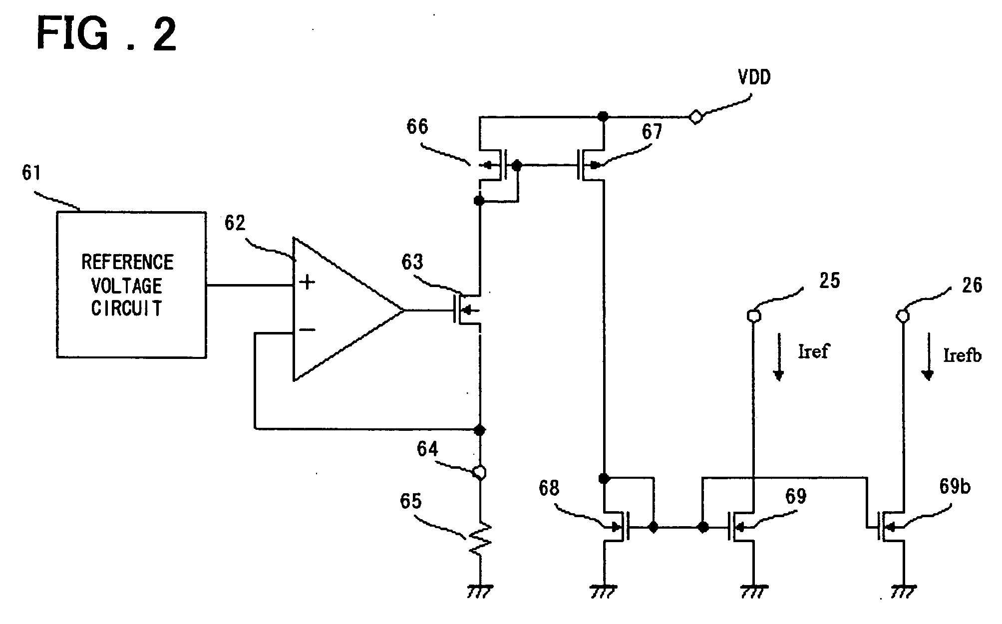
[0027]FIG. 1 is a circuit diagram of a driver circuit according to a first embodiment of the present invention. The driver circuit in FIG. 1 is obtained by adding the temperature characteristic compensating circuit 44 to a driver circuit shown in FIG. 5. The differential pre-buffer circuit 22 is obtained by adding a constant current input terminal 48, N-ch MOS transistors 27 and 28 that constitute a current mirroring current mirror, and a P-ch MOS transistor 29 to a differential pre-buffer circuit 101 in FIG. 5. Further, gates of P-ch MOS transistors 6 and 7 are connected to a drain of a P-ch MOS transistor 29, thereby forming a current mirror. A constant current circuit 24 is a constant current circuit as shown in FIG. 2 and is obtained by adding an N-ch MOS transistor 69b and a current output terminal 26 to a constant current circuit 103 shown in FIG. 6. The differential output circuit 23 is the same as a differential output circuit 102. Since other components in FIG. 1 that have ...
second embodiment
[0033]FIG. 3 is a circuit diagram of a driver circuit according to a second embodiment of the present invention. Referring to the driver circuit in FIG. 3, a temperature characteristic compensation circuit 44a is different from the temperature characteristic compensation circuit 44 in FIG. 1 in that a P-ch MOS transistor 49 is added to the temperature characteristic compensation circuit 44 in FIG. 1. Except that, the temperature characteristic compensation circuit 44a is the same as the temperature characteristic compensation circuit 44 in FIG. 1. Thus, the description will be mainly directed to the P-ch MOS transistor 49. A gate of the P-ch MOS transistor 49 is connected to the gate of the P-ch MOS transistor 33. A drain of the P-ch transistor 49 provides an output of the current mirror of which the P-ch MOS transistor 32 serves as the input side. An output current from the drain of the P-ch MOS transistor 49 is a constant current of which the variations and the temperature variati...
third embodiment
[0038]FIG. 4 is a circuit diagram of a driver circuit according to a third embodiment of the present invention. In a differential pre-buffer circuit 22b and a temperature characteristic compensation circuit 44b in the driver circuit in FIG. 4, the diodes 16, 17 and 43 in FIG. 3 are replaced by N-ch MOS transistors 50, 51, and 52 each with a gate and a drain thereof connected to each other, respectively. Except that, the differential pre-buffer circuit 22b and the temperature characteristic compensation circuit 44b are the same as those in FIG. 3. Thus, their descriptions will be omitted, and the description will be mainly directed to the N-ch MOS transistors 50, 51, and 52.
[0039] Generally, when the gate length is represented by L, and the gate width is represented by W, there is the following relation between the gate-to-source voltage Vgs of an MOS transistor and the drain current Id:
Vgs={(2L / β / W)Id}1 / 2+Vt Equation (15)
in which β=μs×Cox, μs indicates a carrier mobility, Cox i...
PUM
 Abstract
Description
Claims
Application Information