Method of driving memory device to implement multiple states

a memory device and state technology, applied in semiconductor devices, digital storage, instruments, etc., can solve the problems of difficult metal nanocluster formation, difficult miniaturization of chips, and increase of memory chip fabrication costs, and achieve excellent reproducibility

Active Publication Date: 2006-07-20
SAMSUNG ELECTRONICS CO LTD
View PDF5 Cites 22 Cited by
  • Summary
  • Abstract
  • Description
  • Claims
  • Application Information

AI Technical Summary

Benefits of technology

[0012] Accordingly, embodiments of the present invention have been made keeping in mind the above problems occurring in the related art, and an object of embodiments of the present invention is to provide a method of driving a memory device capable of being used as memory having multiple states and having excellent reproducibility, in which the device is driven using multiple pulses to induce a change in resistance.

Problems solved by technology

With respect to this, there is a limit in that the fabrication cost of a memory chip increases as the cost of the above process increases and it is difficult to miniaturize the chip due to this technical limit.
However, this device is problematic in that it is very difficult to form the metal nanoclusters because of very low yield, and it is practically impossible to use it as a nonvolatile memory because of a rest phenomenon at OV voltage.
However, this method is problematic in that, since reproducibility is low, practical usability is doubtful, and transition and switching among the states can be achieved only in a circulation manner.

Method used


Image

  • Method of driving memory device to implement multiple states
  • Method of driving memory device to implement multiple states
  • Method of driving memory device to implement multiple states

Examples


example 1

Fabrication of Test Memory Device

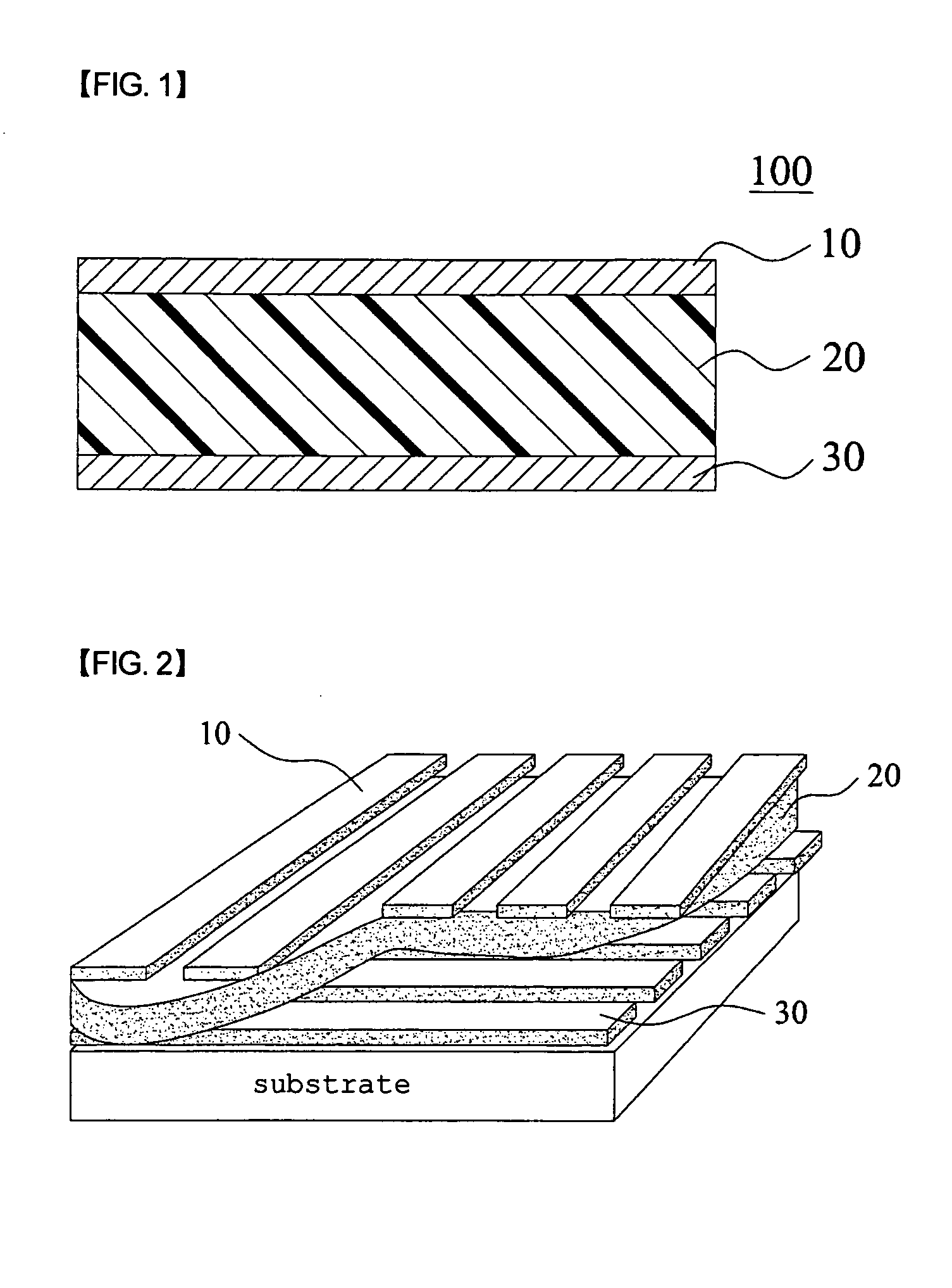
[0045] Aluminum was deposited on a glass substrate using a thermal evaporation method to form a lower electrode, and a barrier layer (Al2O3) was formed to a thickness of 1-2 nm thereon using a spontaneous oxidation method. Subsequently, the barrier layer was coated with a solution in which P3HT was dissolved through a spin coating process, and then baked at 65° C. for 10 min to form an organic memory layer. An Au electrode was deposited as an upper electrode thereon through the thermal evaporation method, thereby fabricating a test device. In this case, the thickness of the organic memory layer was 30 nm and the thickness of the electrodes was 80 nm, measured using an alpha-step profilometer. The thickness of the deposited electrode was controlled using a quartz crystal monitor.

example 2

Driving of Test Device to Implement Multiple States

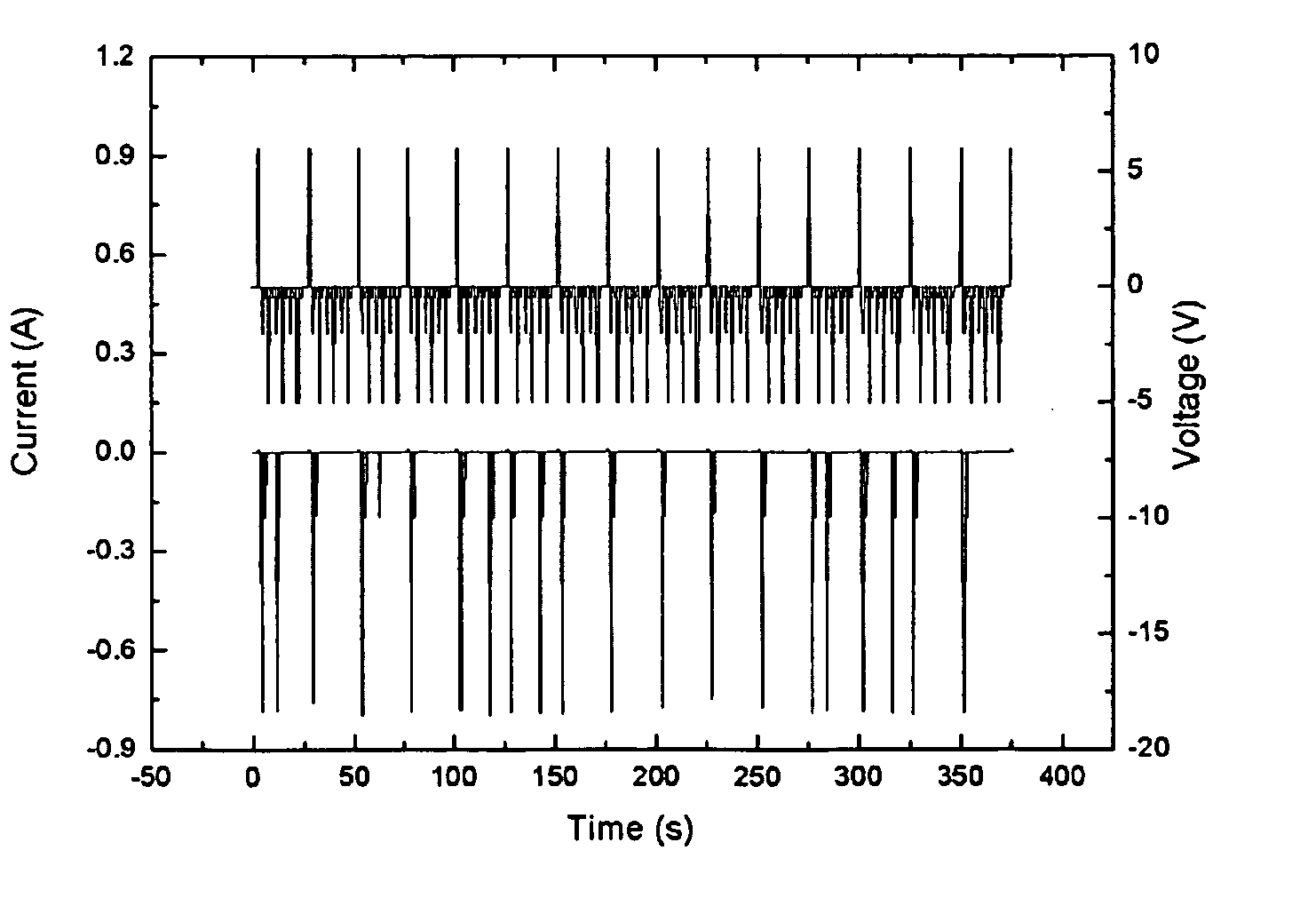
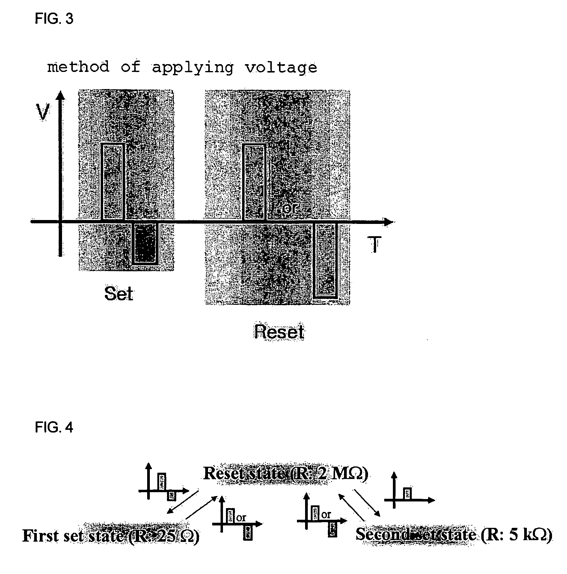
[0046] Current-voltage (I-V) characteristics of a test device, which was driven according to a method of embodiments of the present invention, were measured, and the results are shown in FIG. 7a. Referring to FIG. 7a, a positive voltage pulse of 6.2 V and a negative voltage pulse of −1.7 V were continuously applied to a memory device in a reset state, thereby conducting switching into a low resistance state (a first set). This was confirmed from the observation that a current had a relatively high value when a reading voltage of 1 V was applied. Subsequently, if the negative voltage of −3 V was applied, switching into a reset state was conducted, which was confirmed from the observation that the current had a low value at the reading voltage. FIG. 7b is a graph showing switching employing a negative differential resistance effect caused by driving using a single pulse. Switching from the reset state to a second set state was achiev...

example 3

Test for Duration Time of Switching State of Memory Device

[0047] A memory device of embodiments of the present invention is nonvolatile, which means that information is capable of being stored for a long time. FIG. 8a is a graph showing a duration time in a first set state, and FIG. 8b is a graph showing a duration time in a second set state. In FIGS. 8a and 8b, voltage of 0.05 V was applied to a memory device at room temperature, and a change in the state of the memory device was detected using current. In FIG. 8a, a slight change in current was detected, which meant duration of the first set state, but attenuation was not observed during the detection. On the other hand, in the second state, slight attenuation was observed, and the magnitude of the measured current was small, thus noise occurred. From FIGS. 8a and 8b, it can be seen that it is possible to store information for a long time using the first and second set states.


PUM


Abstract

A method of driving a multi-state organic memory device which includes an organic memory layer between upper and lower electrodes. The method comprises continuously applying voltages having different polarities to conduct switching into a low resistance state, and applying a single pulse to conduct switching into a high resistance state. A multi-state memory is realized using one memory device, since it is possible to gain three or more resistance states, thus significantly improving integration. The method has excellent reproducibility, and the resistance state induced by multiple pulses has an excellent nonvolatile characteristic.

Description

BACKGROUND OF THE INVENTION [0001] This non-provisional application claims priority under 35 U.S.C. § 119(a) on Korean Patent Application No. 2005-5444 filed on Jan. 20, 2005, which is herein expressly incorporated by reference. [0002] 1. Field of the Invention [0003] Embodiments of the present invention relate to a method of driving a memory device to implement multiple states. More particularly, embodiments of the present invention relate to a method of driving a memory device which includes an organic memory layer interposed between upper and lower electrodes so as to implement multiple states, in which switching using multiple pulses and typical switching using negative differential resistance (NDR) are employed to fabricate multi-state memory having at least three different resistance states. [0004] 2. Description of the Related Art [0005] In accordance with recent advances in the information communication industry, demand for various memory devices is rapidly growing. Particul...

Claims


Application Information

Patent Timeline
Patent Type & Authority Applications(United States)
IPC IPC(8): H01L21/336
CPCB82Y10/00G11C11/5664G11C13/0014G11C13/0016G11C2013/0092G11C2013/009G11C2213/77H01L27/285G11C2013/0073G11C13/0069H10K19/202
Inventor JOO, WON JAEKANG, YOON SOKLEE, KWANG HEE
Owner SAMSUNG ELECTRONICS CO LTD
Why Eureka
Try Eureka