Semiconductor device manufacturing method and ion implanter used therein

a technology of semiconductor devices and manufacturing methods, which is applied in the direction of instruments, nuclear engineering, heat measurement, etc., can solve the problems of negative charge-up, implantation produces critical damage on the semiconductor device, and negative charge-up, and achieves reliable neutralization of positive charge-up and suppresses surface potential. rise

Inactive Publication Date: 2006-07-27
PANASONIC CORP
View PDF2 Cites 20 Cited by
  • Summary
  • Abstract
  • Description
  • Claims
  • Application Information

AI Technical Summary

Benefits of technology

[0010] As described above, a flood gun supplies negative electrons for neutralizing the positive charge-up by the ion beam in general. Nevertheless, the electron flood gun, which causes the negative charge-up, produces damage on the semiconductor devices according to the conditions. In this connection, Patent Document 2 discloses that when an electron flood gun that can control the energy of electrons at 2d [eV] or lower is used wherein d is the thickness [nm] of a gate insulating film, damage by the electron flood gun can be mitigated. Hence, the use of the electron flood gun disclosed in Patent Document 2 can prevent at least excessive negative charge-up by the electron flood gun regardless of the device construction.
[0019] The present invention has its object of preventing dielectric breakdown and damages on an insulating film by solving the above conventional problems and suppressing the positive charge-up in a semiconductor device formed on a semiconductor substrate in any scan methods and at any scanning speeds of an ion beam.
[0022] In the semiconductor device manufacturing method of the present invention, the pulse width of the pulsed ion beam is adjusted, so that the irradiation time during which the ion beam is irradiated onto the surface of the semiconductor region can be controlled independently. Accordingly, the positive charge-up can be suppressed in any scan methods and at any scanning speeds of the beam. In turn, the positive charge-up can be neutralized reliably by, for example, an electron flood gun, preventing dielectric breakdown and damage on the insulating film in the case where the insulating film is a capacitor insulating film.
[0023] In the semiconductor device manufacturing method according to the present invention, the insulating film is preferably a capacitor insulating film. Further, the insulating film is preferably a gate insulating film. This prevents damage on the insulating film thinned in association with miniaturization of semiconductor elements.
[0031] In the first ion implanter, the ion beam is irradiated intermittently onto the surface of a to-be-irradiated substance. This suppresses rise in surface potential of the to-be-irradiated substance, enabling reliable neutralization of the positive charge-up by an electron flood gun. As a result, in the case where a capacitor insulating film is formed in the to-be-irradiated substance, dielectric breakdown and damage on the capacitor insulating film can be prevented.
[0039] In the second ion implanter, the ion beam is irradiated intermittently onto the surface of a to-be-irradiated substance. This suppresses rise in surface potential of the to-be-irradiated substance, enabling reliable neutralization of the positive charge-up by an electron flood gun. As a result, in the case where a capacitor insulating film is formed in the to-be-irradiated substance, dielectric breakdown and damage on the capacitor insulating film can be prevented.

Problems solved by technology

The present inventors have found that the positive charge-up by the ion beam in ion implantation produces critical damage on the semiconductor devices such as degradation or dielectric breakdown of the gate insulating films, degradation or junction breakdown of PN junctions, and the like.
Nevertheless, the electron flood gun, which causes the negative charge-up, produces damage on the semiconductor devices according to the conditions.

Method used


Image

  • Semiconductor device manufacturing method and ion implanter used therein
  • Semiconductor device manufacturing method and ion implanter used therein
  • Semiconductor device manufacturing method and ion implanter used therein

Examples


embodiment 1

[0054] Embodiment 1 of the present invention will be described below with reference to the drawings.

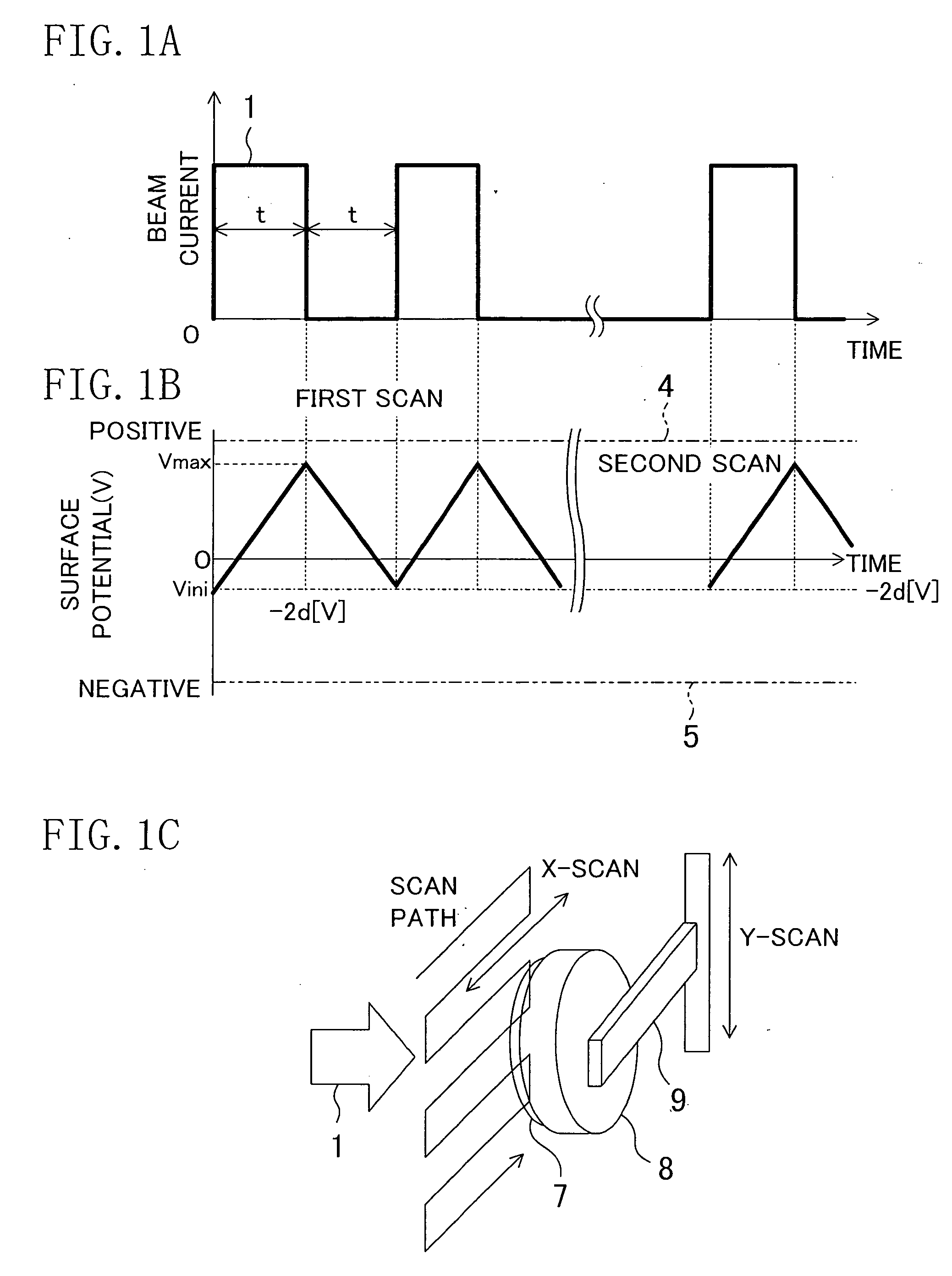
[0055]FIG. 1A shows current-time dependency of a pulsed ion beam used in a semiconductor device manufacturing method according to Embodiment 1 of the present invention, and FIG. 1B shows potential change at the surface of a semiconductor element formed on a semiconductor wafer in a case employing an ion implantation method in the semiconductor device manufacturing method according to Embodiment 1 of the present invention. The surface potential of a gate electrode in a MOS transistor including a gate insulating film having a thickness of 2.0 nm and made of silicon oxide (SiO2) is indicated as the semiconductor element herein.

[0056] In irradiation of an intermittent ion beam 1 having a pulse width t as shown in FIG. 1A to the MOS transistor, the surface potential Vini of the gate electrode is negatively charged up once by electrons (not shown) output from an electron flood gun and sur...

embodiment 2

[0070] Embodiment 2 of the present invention will be described below with reference to the drawings.

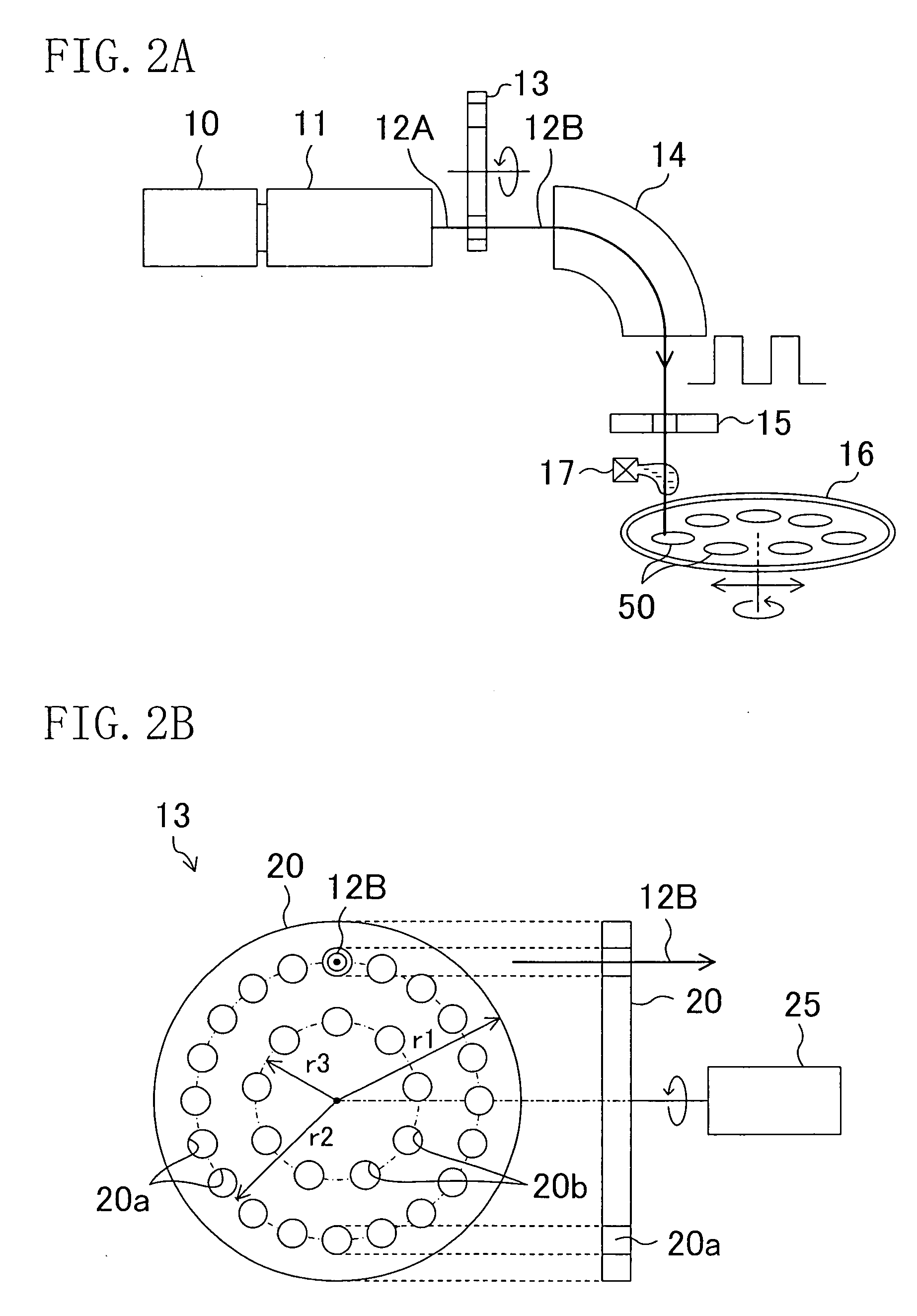
[0071]FIG. 2A schematically shows the main part of an ion implanter according to Embodiment 2 of the present invention, which realizes the method for manufacturing a semiconductor device according to Embodiment 1.

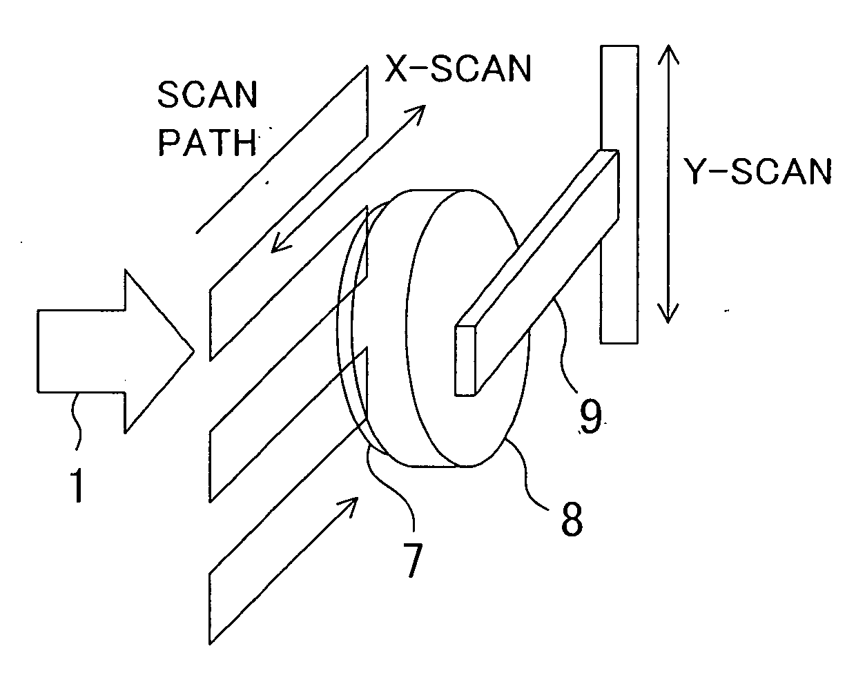
[0072] As shown in FIG. 2A, the ion implanter according to Embodiment 2 includes: an ion source 10 that generates ions to be implanted into semiconductor wafers 50 as impurity ions; an extraction accelerator 11 capable of extracting a continuous ion beam 12A from the ion source 10; a beam shield 13 that generates an intermittent pulsed ion beam 12B from the extracted continuous ion beam 12A; a mass spectrometer 14 that discriminates a predetermined ion species from the generated intermittent ion beam 12B; a beam slit 15 that introduces the discriminated ions into the semiconductor wafers 50; and a rotary disk 16 on which a plurality of wafers 50 are placed and which rotates...

first modified example of embodiment 2

[0086] The first modified example of Embodiment 2 will be described below with reference to the drawing.

[0087]FIG. 4 schematically shows the main part of an ion implanter according to the first modified example of Embodiment 2 of the present invention which realizes the semiconductor device manufacturing method according to Embodiment 1. In FIG. 4, the same reference numerals are assigned to the same constitutional members as those shown in FIG. 2A and the description thereof is omitted.

[0088] In the ion implanter according to the first modified example, the beam shield 13 is arranged between the mass spectrometer 14 and the beam slit 15. Further, as a mechanism for irradiating the intermittent pulsed ion beam 12B to the semiconductor wafer 50, an electrostatic scan electrode 18 capable of magnetically changing the advancing direction of the pulsed ion beam 12B is provided between the beam slit 15 and the semiconductor wafer 50, rather than the rotary disk 16 that rotates the plur...


PUM


Abstract

Impurity ions are implanted into a semiconductor wafer of which a capacitor insulting film is formed on a principal face. In this impurity ion implantation step, the impurity ions are implanted into the semiconductor wafer in the form of a pulsed beam that repeats ON-OFF operation intermittently.

Description

CROSS REFERENCE TO RELATED APPLICATIONS [0001] This Non-provisional application claims priority under 35 U.S.C. § 119(a) on Patent Application No. 2005-17327 filed in Japan on Jan. 25, 2005, the entire contents of which are hereby incorporated by reference. BACKGROUND ART [0002] The present invention relates to a semiconductor device manufacturing method and an ion implanter used therein, and more particularly relates to method for manufacturing a semiconductor device that includes a capacitor insulating film to which ion implantation is performed. [0003] Recently, gate insulating films become thinner in association with miniaturization of elements in semiconductor devices, and therefore, liabilities for damage and dielectric breakdown of the gate insulating films by charge-up in process increase. Among of all, charge-up caused by plasma etching, plasma CVD, and ion implantation presents significant problems in process. [0004] Referring to the ion implantation, an ion beam electrifi...

Claims


Application Information

Patent Timeline
Patent Type & Authority Applications(United States)
IPC IPC(8): H01L21/265H01J37/317
CPCH01J37/3023H01J37/3171H01J2237/0044H01J2237/043
Inventor YONEDA, KENJINIWAYAMA, MASAHIKO
Owner PANASONIC CORP
Why Eureka
Try Eureka