Chemical vapor deposition of chalcogenide materials

a technology of chalcogenide and chemical vapor deposition, which is applied in the direction of chemical vapor deposition coating, liquid surface applicator, coating, etc., can solve the problem that the use of the ovonic family of optical and electrical chalcogenide materials is virtually non-existen

Inactive Publication Date: 2006-08-03
OVONYX
View PDF6 Cites 227 Cited by
  • Summary
  • Abstract
  • Description
  • Claims
  • Application Information

AI Technical Summary

Benefits of technology

[0006] Chemical vapor deposition, hereinafter referred to as CVD, is a widely used technique for the synthesis of materials. In the CVD process, precursors of the constituent elements of a material are reacted to produce a thin film on a substrate. The reaction of the CVD precursors occurs either homogeneously in the gas phase or heterogeneously at the solid-gas interface of the substrate surface. Precursors for many elements are available and a variety of thin film compositions can be synthesized using CVD.

Problems solved by technology

Although CVD, has been widely used for II-VI materials that contain chalcogenide elements and simple binary chalcogenides such as Sb2Te3, its use for the Ovonic family of optical and electrical chalcogenide materials has been virtually non-existent due to the anticipated difficulties associated with producing the multiple element (ternary and higher) compositions typically associated with the most effective optical and electrical switching and memory chalcogenide materials.

Method used


Image

  • Chemical vapor deposition of chalcogenide materials
  • Chemical vapor deposition of chalcogenide materials
  • Chemical vapor deposition of chalcogenide materials

Examples


example 1

[0057] In this example, the CVD synthesis of Sb2Te3 on a silicon nitride substrate is demonstrated. The CVD reactor includes a substrate mount, multiple precursor inlets for delivering precursors in vapor or gas phase form directly or diluted in a carrier gas as well as separate overhead showerhead and backfill lines for providing background pressure of an inert ambient gas.

[0058] A silicon nitride wafer substrate was placed in a CVD reaction chamber. Tris(dimethylamino)antimony (Sb(N(CH3)2)3)was used as the antimony (Sb) precursor to provide the Sb necessary for film formation. Diisopropyltellurium (Te(CH(CH3)2)2) was used as the tellurium (Te) precursor to provide the Te necessary for film formation. The molecular forms of the two precursors are shown in FIG. 3 herein. Both precursors are liquids at ambient condition and were delivered to the CVD reactor in a vapor phase form through use of a bubbler. The Sb-precursor and the Te-precursor were placed in separate bubblers connecte...

example 2

[0062] In this example, a two layer structure including solid phase layers of Sb2Te3 and Ge is prepared in a CVD process. The deposition was performed on a SiN substrate that was rotated at 50 rpm. The CVD reactor, the Sb-precursor and Te-precursor used in this example are as described in EXAMPLE 1 hereinabove. The Ge-precursor was isobutylgermane, H3Ge(i-C4H9), and has the molecular form shown in FIG. 6 herein. The Ge-precursor is a high vapor pressure liquid at ambient conditions and was delivered to the CVD reactor through a bubbler.

[0063] The deposition began with deposition of a Ge layer. The Ge-precursor was placed in a bubbler. 200 sccm of He was bubbled through the Ge-precursor to provide a gas stream containing the Ge-precursor in a vapor phase form in He as a carrier gas. This gas stream was further diluted with 300 sccm of He and then injected into the reactor. During deposition of the Ge layer, 400 sccm He was injected through the showerhead and 250 sccm He was injected...

example 3

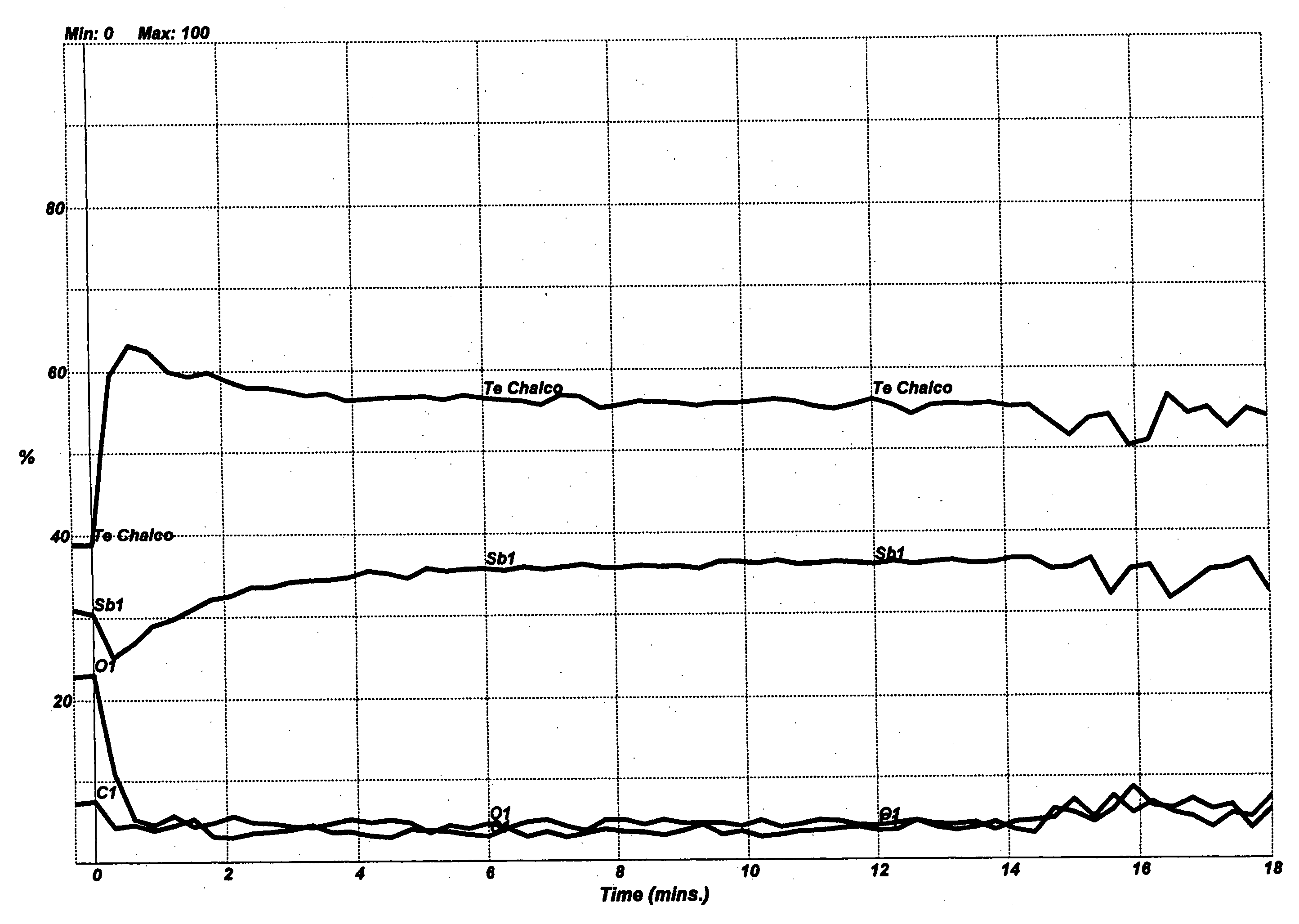
[0073] In this example, a single layer three-element solid phase chalcogenide thin film is deposited by chemical vapor deposition. The deposition was performed on a SiN substrate that was rotated at 50 rpm. The CVD reactor, the Sb-precursor, Te-precursor and Ge-precursor used in this example are as described in EXAMPLE 1 and EXAMPLE 2 hereinabove.

[0074] The deposition in this example was accomplished through a reaction of the Sb-precursor, Te-precursor, and Ge-precursor, where all three precursors were present simultaneously in the CVD reactor. The precursors were introduced into the CVD reactor through separate feed lines. Helium (He) was used as a carrier gas for all three precursors. The Sb-precursor and Te-precursor were placed in separate bubblers heated to 75° C. and delivered to the CVD reactor through separate feed lines, also heated to 75° C. He was bubbled through the Sb-precursor bubbler at a flow rate of 200 sccm to produce a gas stream containing the Sb-precursor in a ...


PUM

PropertyMeasurementUnit
total pressureaaaaaaaaaa
temperatureaaaaaaaaaa
pressureaaaaaaaaaa

Abstract

A chemical vapor deposition (CVD) process for preparing electrical and optical chalcogenide materials. In a preferred embodiment, the instant CVD-deposited materials exhibit one or more of the following properties: electrical switching, accumulation, setting, reversible multistate behavior, resetting, cognitive functionality, and reversible amorphous-crystalline transformations. In one embodiment, a multilayer structure, including at least one layer containing a chalcogen element, is deposited by CVD and subjected to post-deposition application of energy to produce a chalcogenide material having properties in accordance with the instant invention. In another embodiment, a single layer chalcogenide material having properties in accordance with the instant invention is formed from a CVD deposition process including three or more deposition precursors, at least one of which is a chalcogen element precursor. Preferred materials are those that include the chalcogen Te along with Ge and / or Sb.

Description

FIELD OF INVENTION [0001] This invention relates to a process for preparing chalcogenide materials. More particularly, this invention relates to the formation of thin film chalcogenide materials through a metalorganic chemical vapor deposition process. Most particularly, this invention relates to the metalorganic chemical vapor deposition of chalcogenide materials comprising Ge, Sb and Te. BACKGROUND OF THE INVENTION [0002] Chalcogenide materials are materials that contain a chalcogen element (O, S, Se, Te) and typically one or more additional elements that serve to modify electronic or structural properties. The II-VI semiconductors (e.g. CdS, ZnTe etc.) are a well-known class of chalcogenide materials. These materials have been widely investigated for their wide bandgap properties and their potential for providing short wavelength light emission for LED and laser applications. Another important class of chalcogenide materials includes the expansive series of chalcogenide materials...

Claims


Application Information

Patent Timeline
Patent Type & Authority Applications(United States)
IPC IPC(8): C23C16/00B05D1/36B29C71/04
CPCC23C16/305H01L45/04H01L45/06H01L45/144H01L45/1616H10N70/231H10N70/20H10N70/8828H10N70/023H10N70/8825
Inventor OVSHINSKY, STANFORD R.KAMEPALLI, SMURUTHI
Owner OVONYX
Why Eureka
Try Eureka