Illumination optical system, exposure apparatus, and device manufacturing method

an optical system and exposure technology, applied in the field of illumination optical systems, can solve the problems of destroying the degree of vacuum in the vacuum area, enlarge the exposure apparatus and thus not be realistic, and cannot provide an arbitrary and continuous illumination condition

Inactive Publication Date: 2006-08-10
CANON KK
View PDF12 Cites 72 Cited by
  • Summary
  • Abstract
  • Description
  • Claims
  • Application Information

AI Technical Summary

Problems solved by technology

However, those configurations which arrange plural aperture stops on the turret and switch plural integrators provide only a few illumination conditions available, and thus cannot provide an arbitrary and continuous illumination condition.
While the number of available illumination conditions can be increased by increasing the number of aperture stops and the number of integrators, this measure would enlarge the exposure apparatus and thus not be realistic.
The large actuator has a large surface area, emits a large amount of gas, and destroys the degree of vacuum in the vacuum area.
Moreover, in exchanging the aperture stop mounted on the turret etc. from the outside of the vacuum area, the vacuum purge is destroyed once and the atmosphere is opened to the air before the exchange operation starts.
This procedure extremely lowers the operating efficiency of the exposure apparatus.

Method used


Image

  • Illumination optical system, exposure apparatus, and device manufacturing method
  • Illumination optical system, exposure apparatus, and device manufacturing method
  • Illumination optical system, exposure apparatus, and device manufacturing method

Examples


first embodiment

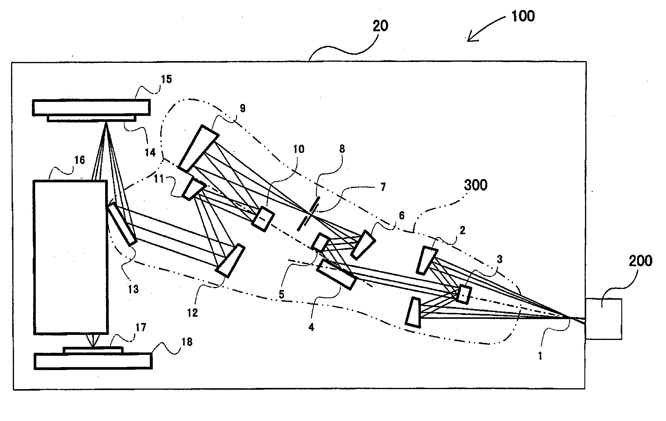
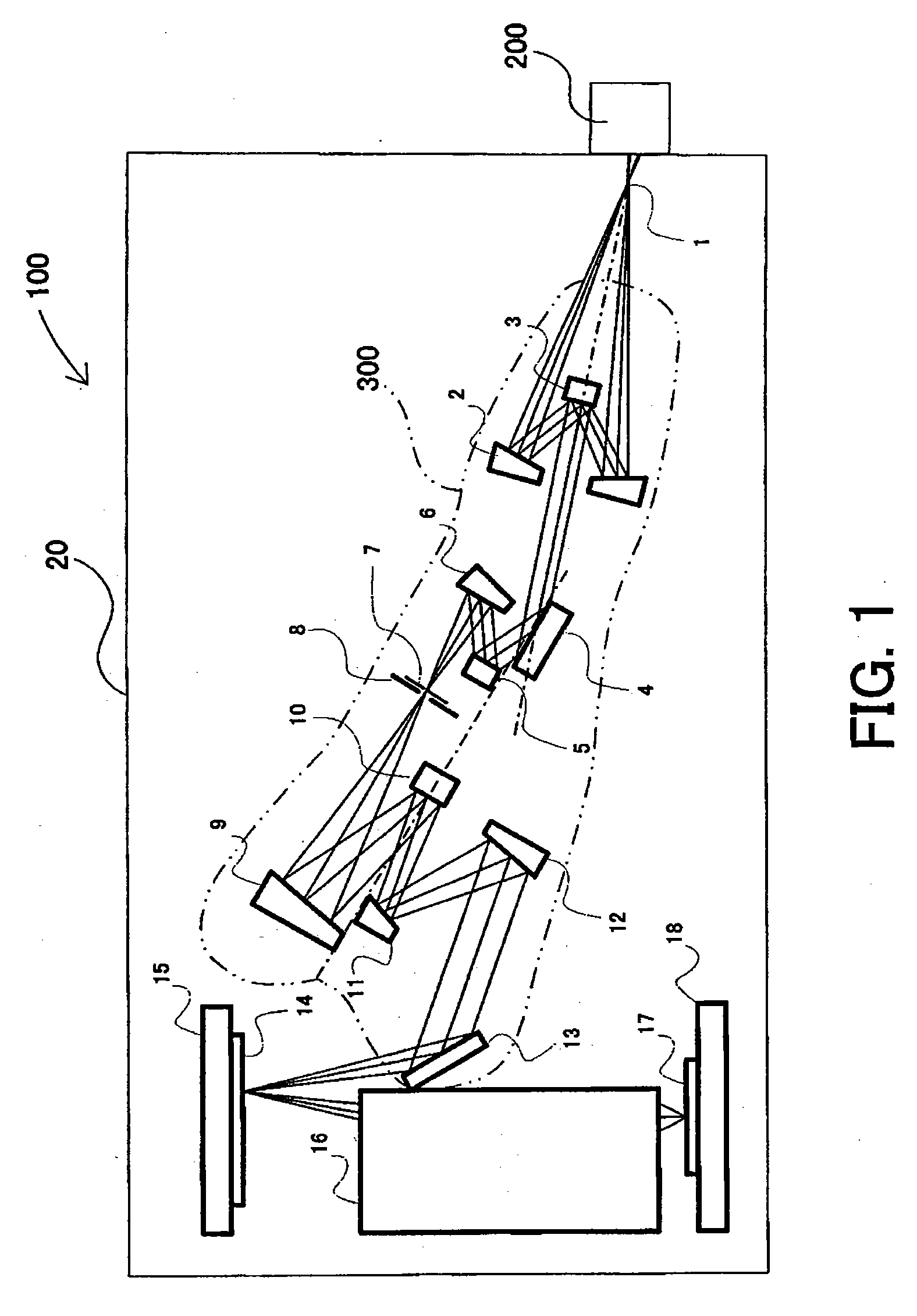
[0022]FIG. 1 shows a schematic structure of a semiconductor exposure apparatus that includes an illumination optical system according to a first embodiment of the present invention. The exposure apparatus 100 of this embodiment is a projection exposure apparatus that provides step-and-scan exposure using the EUV light that has, for example, a wavelength of 13.4 nm, as an illumination light for exposure.

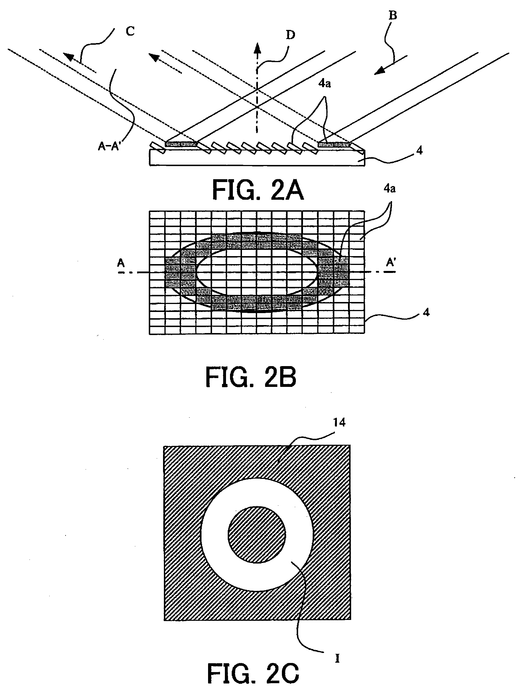
[0023] The exposure apparatus includes a light source section 200, an illumination optical system 300, a reflection type reduction projection optical system 16, a mask stage 15 that holds a reflection mask (or reticle) 14 as an original, and a wafer stage 18 that holds a semiconductor wafer 17 as a substrate to be exposed. The mask stage 15 and the wafer stage 18 are connected to a controller (not shown) so that the controller can control their driving. The mask stage 15 positions the mask 14, and the wafer stage 18 positions the wafer 17. The light source section 200 and the illumin...

second embodiment

[0051] Referring now to FIGS. 7 and 8, a description will be given of an embodiment of a device manufacturing method using the above exposure apparatus 100 according to the first embodiment.

[0052]FIG. 7 is a flowchart for explaining how to fabricate devices (i.e., semiconductor chips such as IC and LSI, LCDs, CCDs, and the like). Here, a description will be given of the fabrication of a semiconductor chip as an example.

[0053] Step 1 (circuit design) designs a semiconductor device circuit. Step 2 (mask fabrication) forms a mask 14 having a designed circuit pattern. Step 3 (wafer preparation) manufactures a wafer 17 using materials such as silicon.

[0054] Step 4 (wafer process), which is also referred to as a pretreatment, forms actual circuitry on the wafer 17 through lithography using the mask 14 and wafer 17.

[0055] Step 5 (assembly), which is also referred to as a posttreatment, forms into a semiconductor chip the wafer 17 formed in Step 4 and includes an assembly step (e.g., di...


PUM


Abstract

An illumination optical system for illuminating a target plane by using light from a light source includes plural displaceable mirrors that are two-dimensionally arranged at specific positions in said illumination optical system.

Description

BACKGROUND OF THE INVENTION [0001] The present invention generally relates to an illumination optical system, and more particularly to an illumination optical system, an exposure apparatus and a device manufacturing method, which use extreme ultraviolet (“EUV”) light having a wavelength between 5 nm and 20 nm to expose a substrate, such as a single crystal substrate for a semiconductor wafer, and a glass plate for a liquid display device (“LCD”). [0002] The conventional illumination optical system in a semiconductor exposure apparatus enables an optical element, such as a lens, to be moved along an optical-axis direction in changing an illumination condition, such as a coherence factor σ (a ratio between the numerical aperture (“NA”) of the illumination optical system at the mask side and the NA of the projection optical system at the mask side) in a normal illumination, and a shape of a off-axis illumination, e.g., an annular ratio in the annular illumination (a ratio between an in...

Claims


Application Information

Patent Timeline
Patent Type & Authority Applications(United States)
IPC IPC(8): G21G5/00A61N5/00
CPCG03F7/70116G03F7/70133G03F7/702G21K1/06
Inventor YABUKI, AKIRA
Owner CANON KK
Why Eureka
Try Eureka