Switched capacitor circuit and semiconductor integrated circuit thereof

a technology of semiconductor integrated circuits and capacitors, which is applied in the direction of time-varying networks, transistors, solid-state devices, etc., can solve the problems of large fluctuation width of output voltage, and generation of noise during switching

Inactive Publication Date: 2006-08-17
OHMI +1
View PDF4 Cites 12 Cited by
  • Summary
  • Abstract
  • Description
  • Claims
  • Application Information

AI Technical Summary

Benefits of technology

[0020] The present invention aims at reducing the error of a switched capacitor circuit, and also aims at reducing the noise and the voltage fluctuation during switching.

Problems solved by technology

When a p-channel MOS transistor and an n-channel MOS transistor are connected in parallel and used as a switch of a switched capacitor circuit, a problem occurs; noise is generated during switching because the parasitic capacity of the p-channel MOS transistor is different from the parasitic capacity of the n-channel MOS transistor.
When a switched capacitor filter is formed on the substrate of the integrated circuit, there is the problem that a filter characteristic based on the designed value cannot be obtained due to the leak current of a transistor and the offset voltage of an operational amplifier.
Furthermore, when a CMOS switch is used, there has been the problem that the fluctuation width of an output voltage is large when the switch is turned to the on and off positions because the parasitic capacity of the p-channel MOS transistor is larger than the parasitic capacity of the n-channel MOS transistor.

Method used


Image

  • Switched capacitor circuit and semiconductor integrated circuit thereof
  • Switched capacitor circuit and semiconductor integrated circuit thereof
  • Switched capacitor circuit and semiconductor integrated circuit thereof

Examples


Embodiment Construction

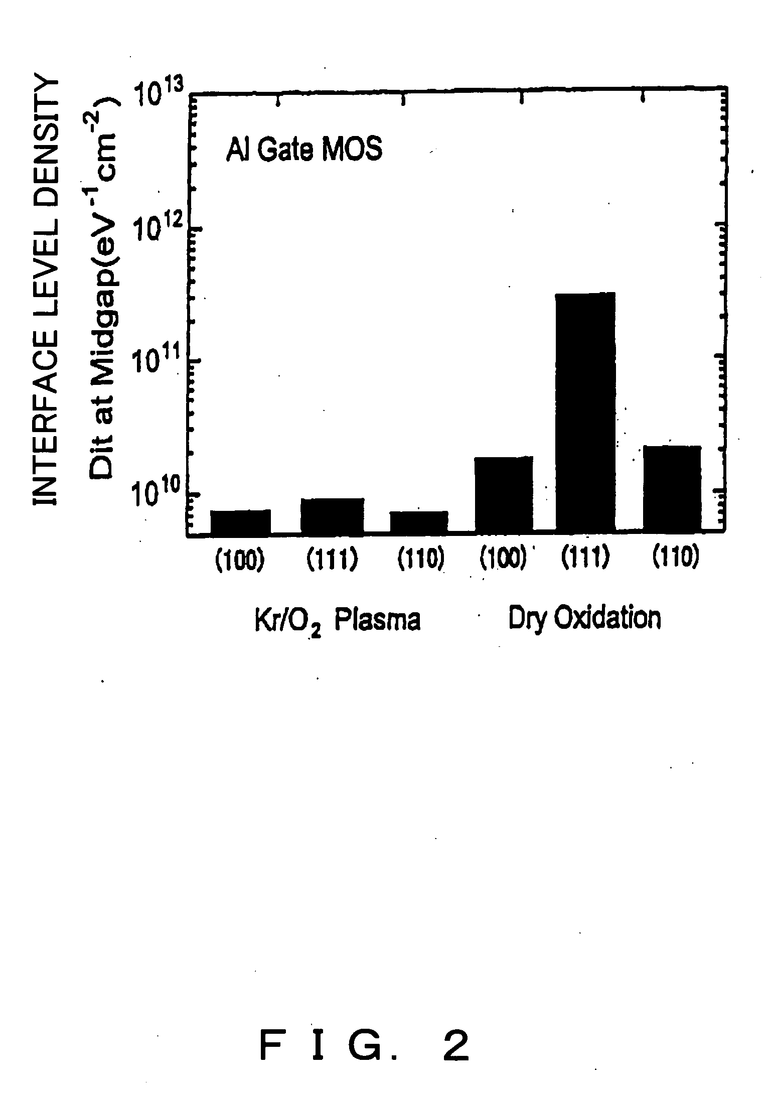
[0048] An embodiment of the present invention is explained below by referring to the attached drawings. Described below is a semiconductor production process of forming a gate insulating film (for example, an oxide film) on the silicon substrate at a low temperature using an inert gas in a plasma state, and producing a MIS (metal insulator semiconductor) field-effect transistor. The method for forming a gate insulating film is disclosed in Japanese Published Patent Application No. 2002-261091.

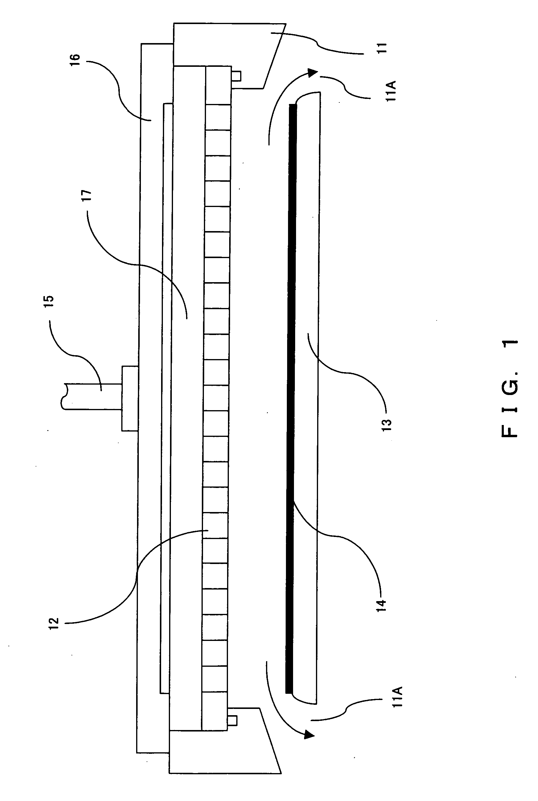
[0049]FIG. 1 is a sectional view of the plasma device using a radial line slot antenna to be used in the semiconductor producing process.

[0050] A vacuum is produced in a vacuum container (processing chamber) 11, argon gas (Ar) is introduced from a shower plate 12, the Ar gas is exhausted from an outlet 11A, and the gas is switched to a krypton gas. The pressure in the processing chamber 11 is set to 133 Pa (1 Torr).

[0051] Then, a silicon substrate 14 is placed on a sample table 13 having a h...


PUM


Abstract

A rectangular parallelepiped projecting portion (21) having a height of HB and a width of WB is formed on a silicon substrate, and a gate oxide film is formed on a part of the top surface and the side surface of the projecting portion (21), thereby generating a MOS transistor. By connecting in parallel a p-channel MOS transistor and an n-channel MOS transistor produced as described above, a switch of a switched capacitor circuit is configured, thereby reducing a leak current and a DC offset of the switched capacitor circuit.

Description

TECHNICAL FIELD [0001] The present invention relates to a switched capacitor circuit formed on the substrate of a semiconductor integrated circuit, and a semiconductor integrated circuit including the switched capacitor circuit. BACKGROUND ART [0002] Conventionally, in the production process of a MOS transistor, a thermal oxide film is formed on the silicon surface at a high temperature of 800° C. as a gate insulating film. [0003] It is requested to form an oxide film at a lower temperature environment to enhance the production efficiency of a semiconductor. To realize this request, for example, the patent document 1 discloses the technology of forming an insulating film in a low temperature plasma atmosphere. [0004] When a filter is formed on the substrate of an integrated circuit, a switched capacitor filter is used. [0005] When a p-channel MOS transistor and an n-channel MOS transistor are connected in parallel and used as a switch of a switched capacitor circuit, a problem occur...

Claims


Application Information

Patent Timeline
Patent Type & Authority Applications(United States)
IPC IPC(8): H01L29/94H01L27/108H01L29/76H01L31/119H01L21/336H01L21/8238H01L27/092H03H19/00
CPCH01L21/823807H01L21/82385H01L27/092H01L29/66787H01L27/00
Inventor NISHIMUTA, TAKEFUMIMIYAGI, HIROSHIOHMI, TADAHIROSUGAWA, SHIGETOSHITERAMOTO, AKINOBU
Owner OHMI
Why Eureka
Try Eureka