Electroluminescent device and display

a technology of electroluminescent devices and displays, applied in the direction of discharge tubes/lamp details, discharge tubes/lamp details, cathode ray tubes/electron beam tubes, etc., can solve the problems of low luminous efficiency and brightness, difficulty in increasing the size of one semiconductor substrate, and increasing the manufacturing cost proportional to the number of elements, etc., to achieve high brightness, low voltage drive, and high luminous efficiency

Inactive Publication Date: 2006-08-17
PANASONIC CORP
View PDF10 Cites 26 Cited by
  • Summary
  • Abstract
  • Description
  • Claims
  • Application Information

AI Technical Summary

Benefits of technology

[0026] As described above, according to the electroluminescent element of the present invention, a wide band-gap semiconductor performs ultraviolet region luminescence or blue light luminescence with a low voltage, and the phosphor is excited by the short wavelength light thereof, so the phosphor layer emits light as a whole. Therefore, high brightness and high luminous efficiency can be obtained. Further, since the matrix consists of a transparent conductor, the flow of electrons continues, whereby a low voltage drive (low power consumption) and a long lifetime are realized. Further, an increase in size is easily realized, whereby a cost reduction can be achieved.

Problems solved by technology

However, they must be formed on a compound semiconductor substrate, and it is difficult to increase the size of one semiconductor substrate.
This causes a problem of an increase in the manufacturing cost in proportion to the number of elements.
However, the luminous efficiency and brightness are low, and the lifetime is as short as about ten thousands hours, so there are shortcomings practically.
Therefore, it is difficult to perform a drive of active matrix type using general purpose thin film transistors, causing a problem that the cost of driving circuit increases.
Therefore, it is required to apply an AC voltage of several hundreds V in a high frequency of several kHz generally, causing a problem that the cost of the driving circuit increases.

Method used


Image

  • Electroluminescent device and display
  • Electroluminescent device and display
  • Electroluminescent device and display

Examples


embodiment 1

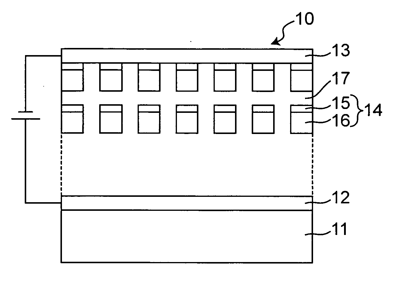
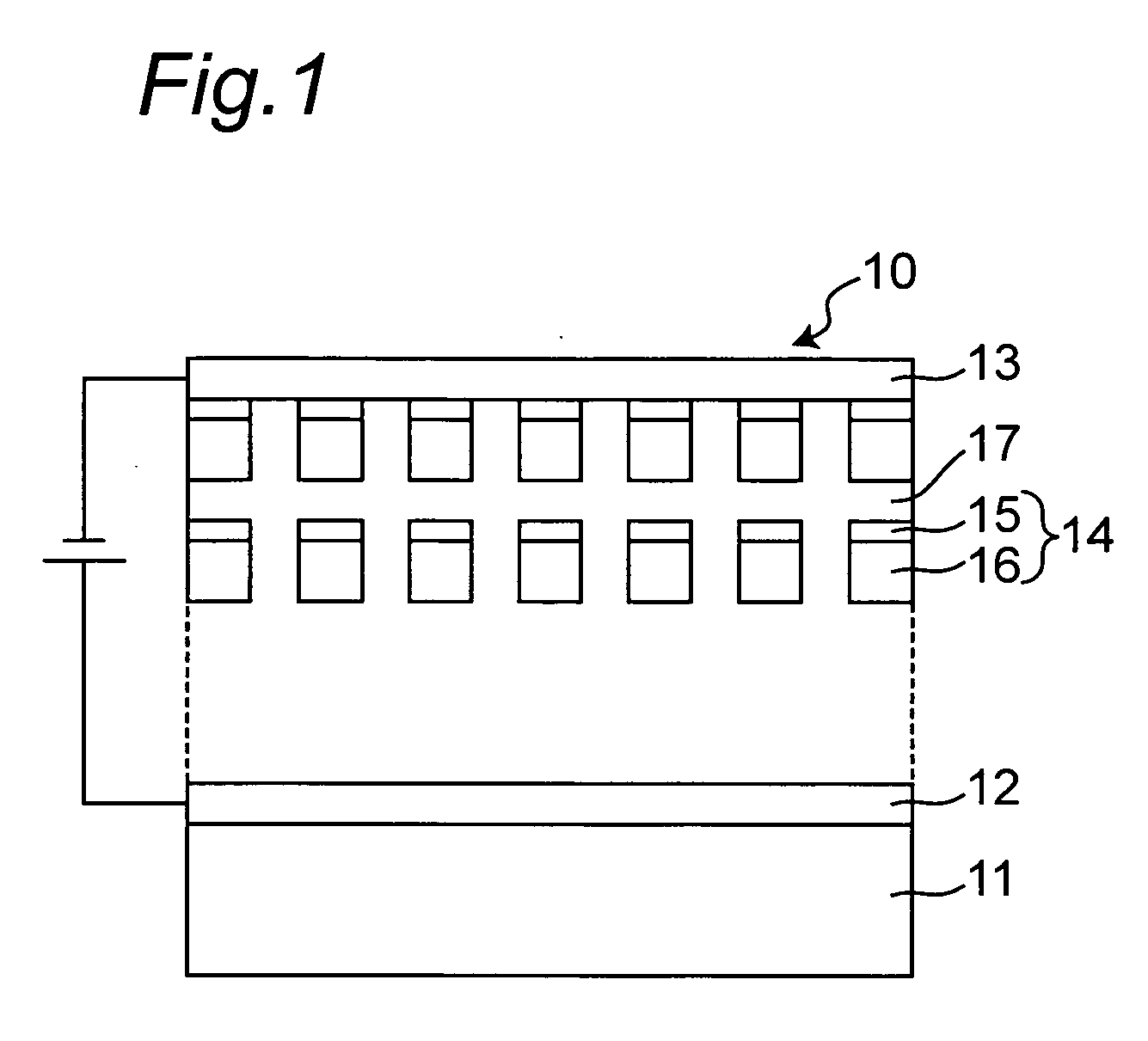
[0044] An electroluminescent element according to an embodiment 1 of the present invention will be explained by using FIG. 1. FIG. 1 is a cross-sectional view showing the configuration of an electroluminescent element 10 according to the embodiment 1. The electroluminescent element 10 has a multi-layer structure, in which a pair of positive electrode 12 and negative electrode 13 facing each other is provided on a substrate 11. Further, in between the positive electrode 12 and the negative electrode 13, a phosphor layer 14 consisting of a semiconductor layer 15 and a phosphor layer 16 is laminated repeatedly via a transparent conductive layer 17. The semiconductor layer 15 and the phosphor layer 16 constituting the phosphor layer 14 is a discontinuous layer, in which discontinuous parts between respective phosphor layers 14 are filled with the transparent conductive layer 17. Note that although only two sets of phosphor layers 14 are described in FIG. 1, the present invention is not ...

embodiment 2

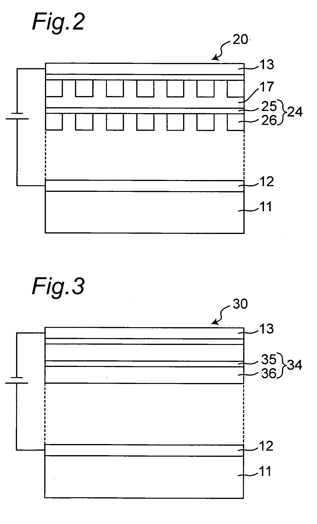
[0052] An electroluminescent element 20 according to an embodiment 2 of the present invention will be described by using FIG. 2. Comparing with the electroluminescent element of the embodiment 1, the electroluminescent element 20 is different in that a semiconductor layer 25 of a wide band-gap constituting a phosphor layer 24 is a continuous layer.

embodiment 3

[0053] An electroluminescent element 30 according to an embodiment 3 will be described by using FIG. 3. Comparing with the electroluminescent element of the embodiment 1, the electroluminescent element 30 is different in that both of a semiconductor layer 35 of a wide band-gap and a phosphor layer 36 constituting a phosphor layer 34 are continuous layers.


PUM


Abstract

An electroluminescent element includes a pair of positive electrode and negative electrode facing each other, and at least one phosphor layers formed between the pair of positive electrode and negative electrode. At least one of the phosphor layers is composed of a phosphor layer and a wide band-gap semiconductor layer. The semiconductor layer or the phosphor layer constituting the phosphor layer may be a partially discontinuous layer.

Description

BACKGROUND [0001] 1. Technical Field [0002] The present invention relates to electroluminescent elements used for a planar light source and a flat display device. [0003] 2. Description of the Related Art [0004] Conventional light emitting devices, used for planar light sources and flat display devices, use light emitting diodes or electroluminescent elements (referred to as EL elements). [0005] Light emitting diodes are advantageous in high brightness and high luminous efficiency. However, they must be formed on a compound semiconductor substrate, and it is difficult to increase the size of one semiconductor substrate. Further, in order to increase the size of a flat display device, a large number of light emitting diodes must be arranged in two dimensions. [0006] The structure of an EL element will be explained by using FIG. 5. FIG. 5 is a cross-sectional view showing the structure of an EL element. An EL element 50 has a cell structure in which a phosphor layer 54 is interposed be...

Claims


Application Information

Patent Timeline
Patent Type & Authority Applications(United States)
IPC IPC(8): H01J1/62
CPCH01J29/26H01J31/127H01J2329/00H05B33/145
Inventor NAGO, KUMIOODAGIRI, MASARUONO, MASAYUKIHORI, KENYA
Owner PANASONIC CORP
Why Eureka
Try Eureka