Semiconductor apparatus and complimentary MIS logic circuit

a logic circuit and semiconductor technology, applied in the direction of semiconductor devices, electrical devices, transistors, etc., can solve the problems of large semiconductor apparatus, high drive power, small threshold voltage of mos transistor, etc., and achieve the effect of reducing power consumption

Inactive Publication Date: 2006-08-24
SOCIONEXT INC
View PDF3 Cites 16 Cited by
  • Summary
  • Abstract
  • Description
  • Claims
  • Application Information

AI Technical Summary

Benefits of technology

[0011] It is therefore an object of the present invention to provide a semiconductor apparatus and complimentary MIS logic circuit configured using this semiconductor apparatus that control the substrate bias voltage using a simple method without a substrate bias application circuit and enable the simultaneous implementation of both high-speed operation and lower power consumption during standby without making substrate potential unstable when a MOS transistor goes on.

Problems solved by technology

However, there is a tendency for sub-threshold leakage current that is unnecessary current flowing between a source and a drain to increase as the threshold voltage is lowered.
This means that the threshold voltage of the MOS transistor becomes small and the drive power becomes high.
However, the method of suppressing the sub-threshold leakage current disclosed in patent document 1 requires a circuit for applying the substrate bias and this causes the semiconductor apparatus to become large and costs to increase.
Further, with the technology disclosed in patent document 2, a pair of signals of normal and reverse phases such as with pass transistor logic are necessary, which means that signal circuits become complex.
This means that if the number of outputs is large, the circuit scale also becomes large.
As a result, when a gate voltage is applied in order to put a MOS transistor ON, cases where a change in substrate potential resulting from the gate capacitance no longer exceeding a clamp voltage VC of a diode constructed from the base and emitter of the BJT occur, and the substrate potential therefore becomes unstable.

Method used


Image

  • Semiconductor apparatus and complimentary MIS logic circuit
  • Semiconductor apparatus and complimentary MIS logic circuit
  • Semiconductor apparatus and complimentary MIS logic circuit

Examples


first embodiment

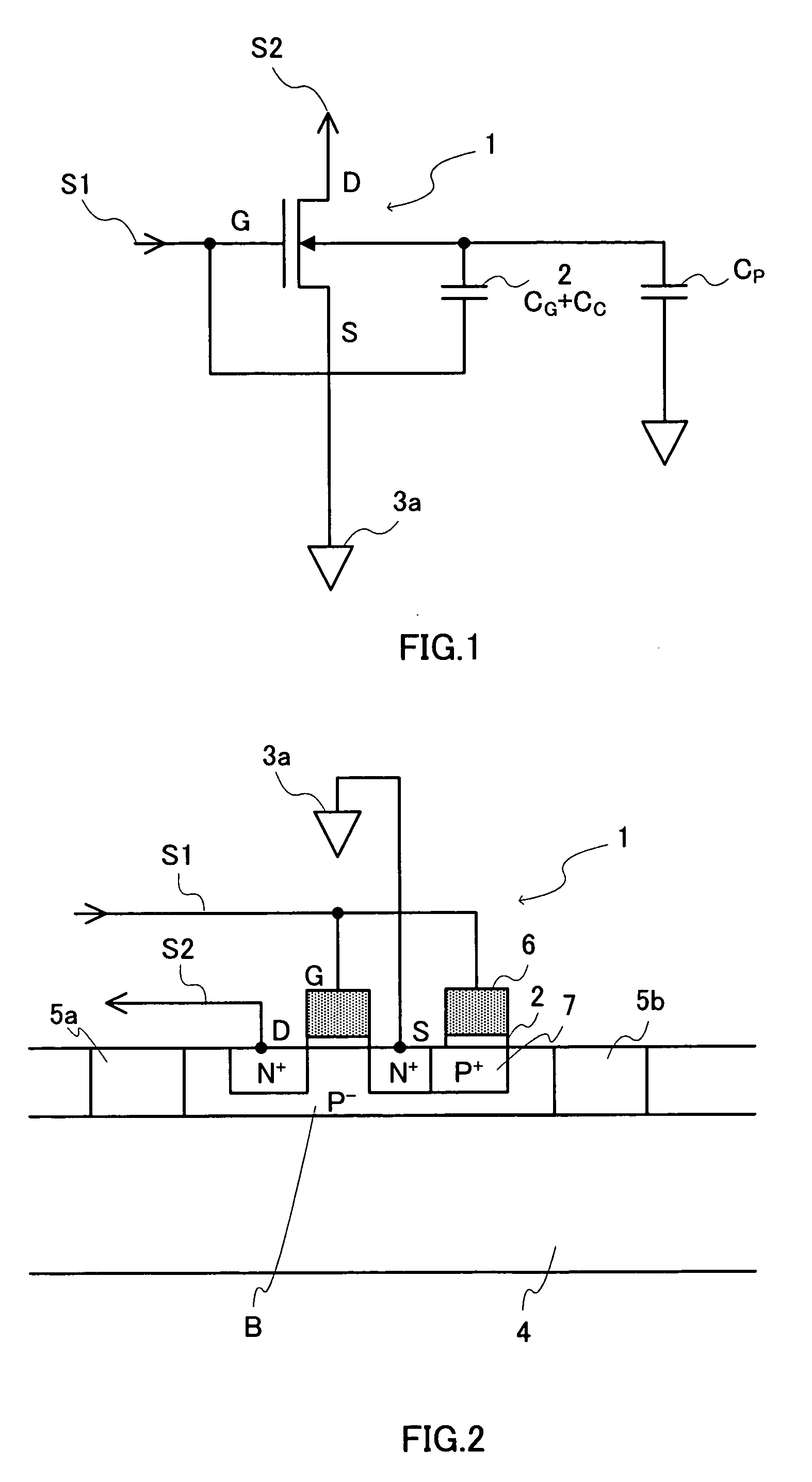
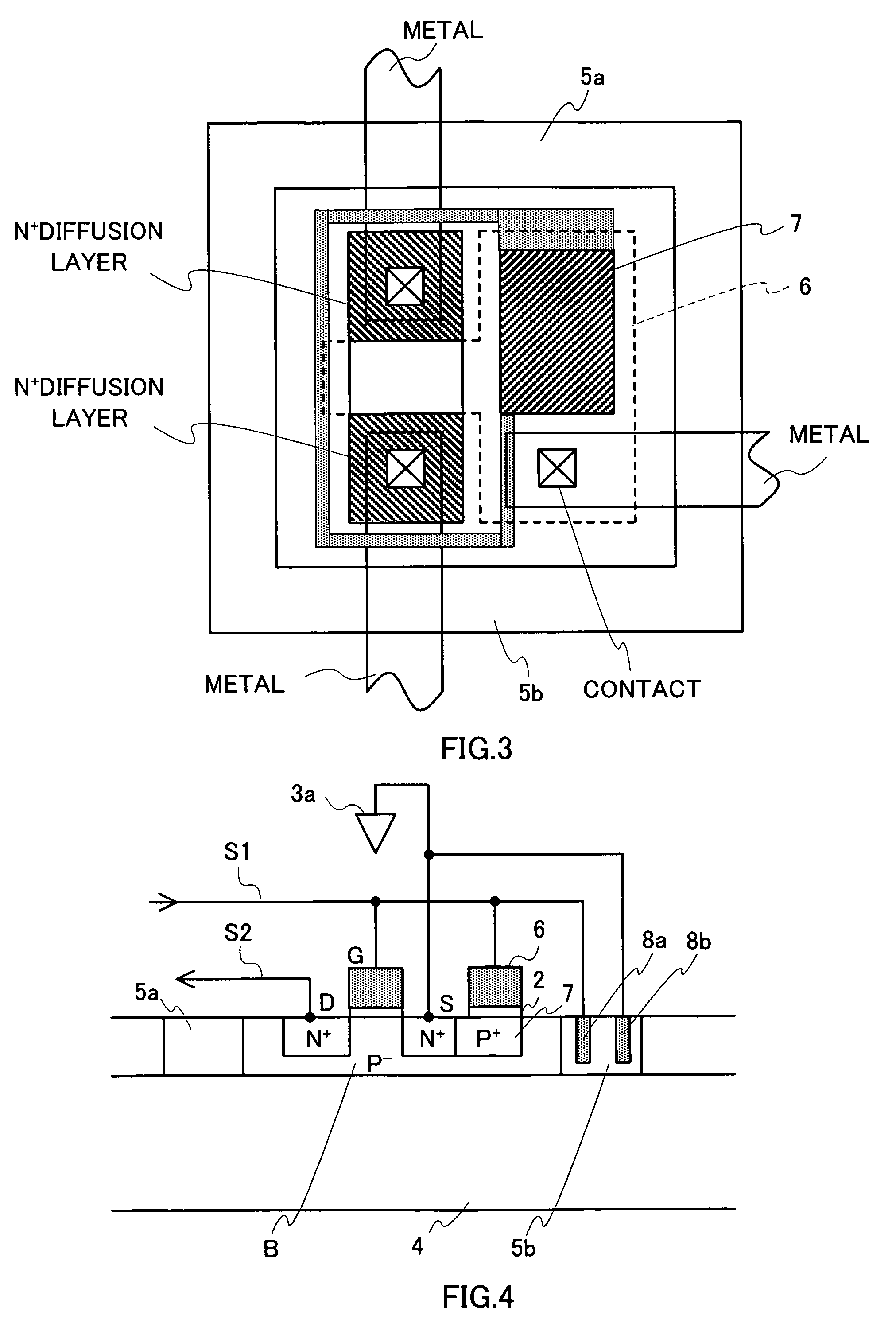
[0033]FIG. 1 is a circuit diagram showing a configuration for an NchMOS-type semiconductor apparatus of a first embodiment of the present invention. Further, FIG. 2 is a schematic cross-sectional view of the NchMOS-type semiconductor apparatus shown in FIG. 1. Moreover, FIG. 3 is a plain view showing an example of a mask drawing for the NchMOS-type semiconductor apparatus shown in FIG. 1. First, a description is given of a circuit configuration for an NchMOS-type semiconductor apparatus corresponding to the first embodiment using FIG. 1 and FIG. 2.

[0034] The NchMOS-type semiconductor apparatus shown in FIG. 1 and FIG. 2 is comprised of a perfectly depleted or close to perfectly depleted partially depleted-type NchMOS transistor 1 formed on a silicon substrate in an electrically insulated and isolated floating state by providing insulating isolation regions 5a, 5b on a silicon substrate equipped with an insulating isolation layer 4 insulated and isolated by an SOI structure, and a c...

second embodiment

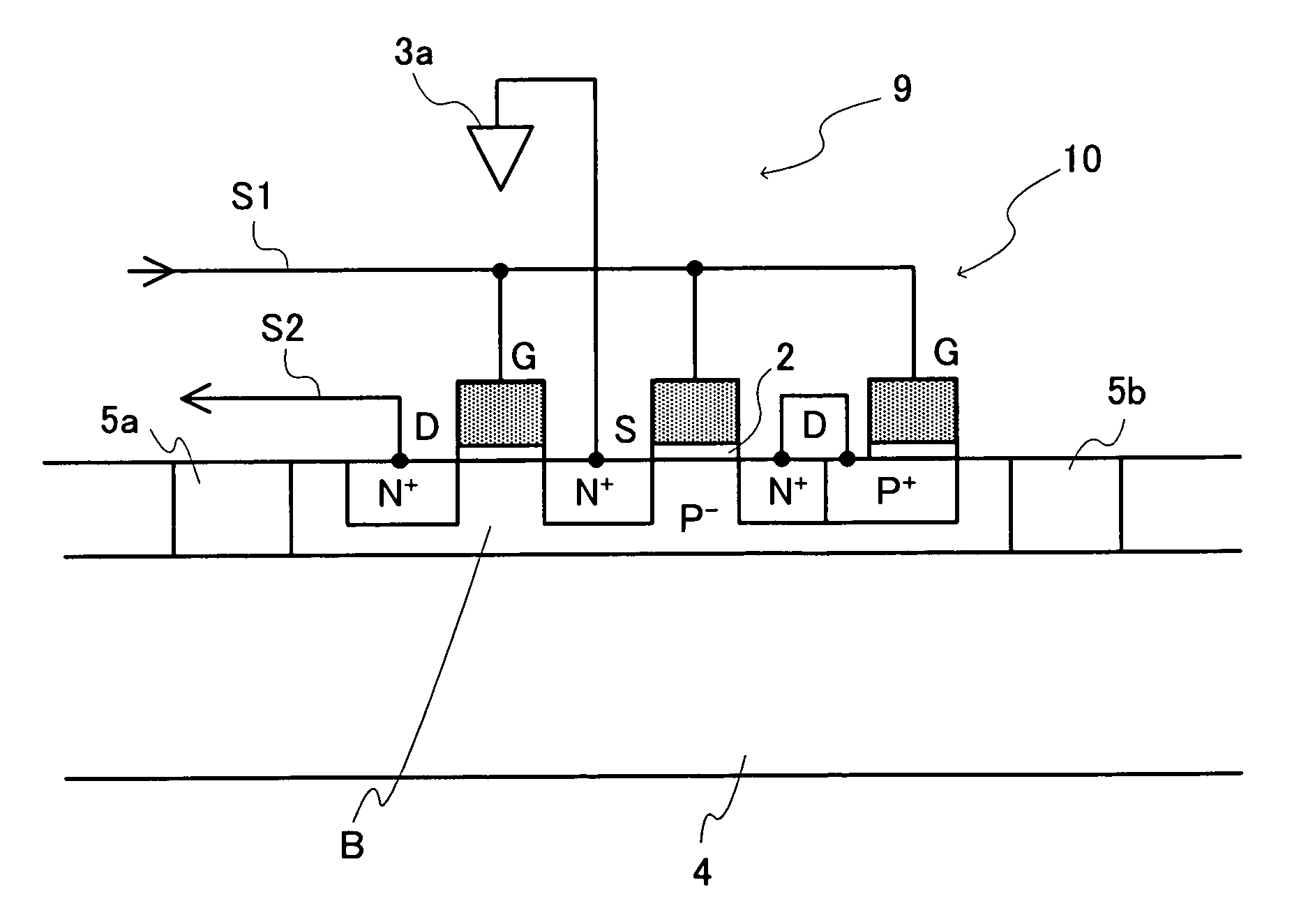
[0044]FIG. 5 is a circuit diagram showing a configuration for an NchMOS-type semiconductor apparatus of a second embodiment of the present invention. Further, FIG. 6 is a schematic cross-sectional view of the NchMOS-type semiconductor apparatus shown in FIG. 5. This NchMOS-type semiconductor apparatus has the same configuration as the NchMOS-type semiconductor shown in FIG. 1 and FIG. 2 and duplicate descriptions are therefore omitted. In the second embodiment shown in FIG. 5, a configuration is adopted where the NchMOS transistor 1 of the first embodiment shown in FIG. 1 is made a NchMOS transistor 9 for logic circuit use, and an NchMOS transistor 10 for substrate potential control use is added between a source electrode S and silicon substrate B of the NchMOS transistor 9 for logic circuit use, and the gate electrodes G of the NchMOS transistor 9 for logic circuit use and the NchMOS transistor 10 for substrate potential control use are connected together.

[0045]FIG. 14 is a view s...

third embodiment

[0046] In a third embodiment, a description is given of a PchMOS-type semiconductor apparatus. FIG. 7 is a circuit diagram showing a configuration for a PchMOS-type semiconductor apparatus of a third embodiment of the present invention. The basic circuit configuration is exactly the same other than the NchMOS-type semiconductor apparatus shown in FIG. 1 being changed to a PchMOS-type semiconductor apparatus. In the case of the PchMOS transistor 11 shown in FIG. 7, when the voltage of the gate electrode G is changed from high to low, the PchMOS transistor 11 changes from an OFF to ON state, and the substrate potential is pushed down in a negative voltage direction by coupling of a capacitor 12, so that a negative substrate potential is generated. The relational expression for the substrate potential is the same as for equation (1) of the first embodiment simply except that the polarity changes. When the voltage for the gate electrode G is changed from low to high, the PchMOS transist...


PUM


Abstract

A configuration is adopted comprising an NchMOS transistor 1 equipped with an insulating isolation layer 4 providing insulation and isolation using an SOI structure, and a capacitor formed using an insulating film, with a silicon substrate B being made thin and substrate capacitance being reduced. The NchMOS transistor 1 is equipped with insulating isolation regions 5a, 5b that are perfectly depleted or partially depleted in a manner close to being perfectly depleted. An electrode 6 connected to a gate electrode G of the NchMOS transistor 1 and an impurity diffusion layer 7 are connected via a capacitor 2. A source electrode S is connected to a power supply terminal 3a, a gate electrode G is connected to an internal signal line S1, and a drain electrode D is connected to an internal signal line S2. Substrate bias voltage is then controlled using capacitor coupling when the NchMOS transistor 1 is turned on/off.

Description

BACKGROUND OF THE INVENTION [0001] 1. Field of the Invention [0002] The present invention relates to an MIS (Metal Insulator Semiconductor) structure semiconductor apparatus made on Silicon On Insulator (SOI). More particularly, the present invention relates to a semiconductor apparatus such as an MOS (Metal Oxide Semiconductor) achieving both high-speed operation and low leakage current, and complimentary MIS logic circuit made using this semiconductor apparatus. [0003] 2. Description of Related Art [0004] In the related art, it is well-known that, in order to make MOS transistors themselves high-speed, in addition to miniaturizing the semiconductor elements and making gate lengths of MOS transistors shorter, lowering threshold voltage is extremely effective. However, there is a tendency for sub-threshold leakage current that is unnecessary current flowing between a source and a drain to increase as the threshold voltage is lowered. Various technology has therefore been reported to...

Claims


Application Information

Patent Timeline
Patent Type & Authority Applications(United States)
IPC IPC(8): H01L27/12
CPCH01L27/1203H01L2924/0002H01L2924/00
Inventor ITO, MINORU
Owner SOCIONEXT INC
Why Eureka
Try Eureka