Electroluminescent devices with electrode protection

a technology of electroluminescent devices and electrode protection, which is applied in the direction of discharge tube/lamp details, discharge tube luminescnet screens, other domestic objects, etc., can solve the problems of exciton confinement, high photoluminescence and electroluminescence efficiency, and observe detrimental effects, so as to facilitate the removal of any interaction with the electrode during conversion. , the effect of reducing the effect of the interaction

Inactive Publication Date: 2006-08-24
CAMBRIDGE DISPLAY TECH LTD
View PDF19 Cites 13 Cited by
  • Summary
  • Abstract
  • Description
  • Claims
  • Application Information

AI Technical Summary

Benefits of technology

[0021] Thus, in another embodiment the electrode protection layer and the precursor polymer is deposited on the cathode, typically a material such as aluminium or an alloy of aluminium with a low work function element or any low work function element or alloy. In this case the protection layer will need to transport electrons, but may or may not need to be transparent. Again conducting polymers are suitable candidates as cathode protection layers. The anode electrode is placed on the other side of the converted precursor material and completes the device structure.
[0022] In yet another embodiment a protection layer to either the anode or cathode as described above is provided but where the protection layer is an undoped conjugated polymer but which has sufficient injection properties and transport mobilities for either holes or electrons depending on whether it is protecting the anode or cathode respectively. An example of such a protection layer would be a soluble PPV derivative or alternatively a precursor PPV or PPV derivative material. In the latter case, if the protection layer is much thinner than the electroluminescence layer, the by-products of the conversion process are more easily removed and therefore any interaction with the electrode during conversion is reduced.
[0024] In yet another embodiment a protection layer to either the cathode or anode as described above is provided, but where the protection layer is an undoped and non-conjugated polymer but which has sufficient injection properties and transport mobilities for either holes or electrons depending on whether it is protecting the anode or cathode respectively. An example would be polyvinyl carbazole which is a good hole transporting material but is not a conjugated polymer. Alternatively very thin layers of polymer materials which have relatively poor hole and electron mobilities may function as good electrode protectors without compromising the balance of electron and hole charge carriers. Examples would be polystyrene and poly (vinyl pyridine).
[0036] an electrode protection layer formed between the electrode and the light-emissive layer so as to protect the electrode during conversion of the organic precursor.

Problems solved by technology

In addition to the observation of quenching via the presence of impurities from the interaction of by-products with indium tin oxide during conversion, we have also observed detrimental effects due to the enhanced conversion of certain PPV copolymers.
This normally leads to exciton confinement and therefore high photoluminescence and electroluminescence efficiencies.

Method used


Image

  • Electroluminescent devices with electrode protection
  • Electroluminescent devices with electrode protection
  • Electroluminescent devices with electrode protection

Examples


embodiment i

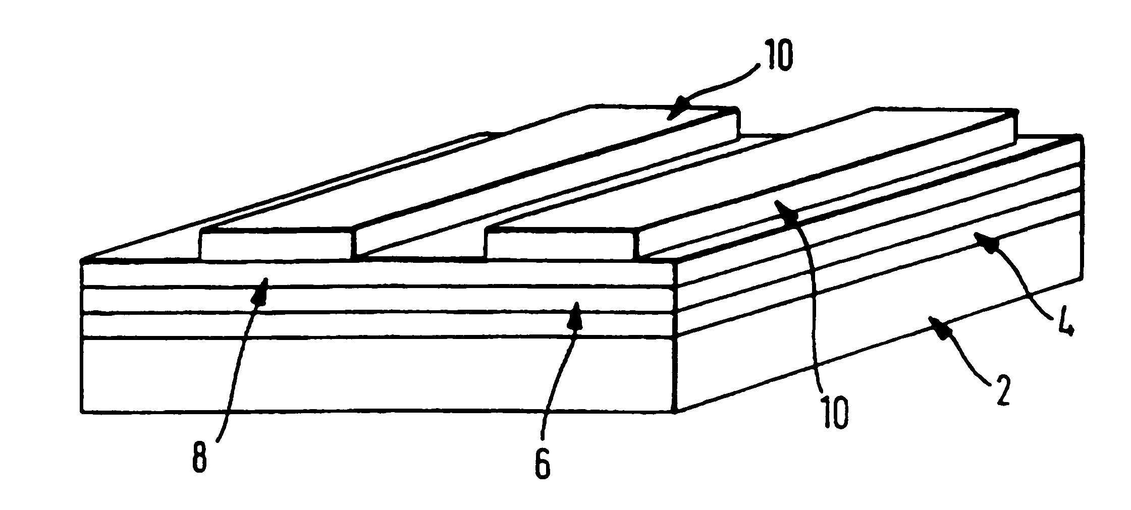
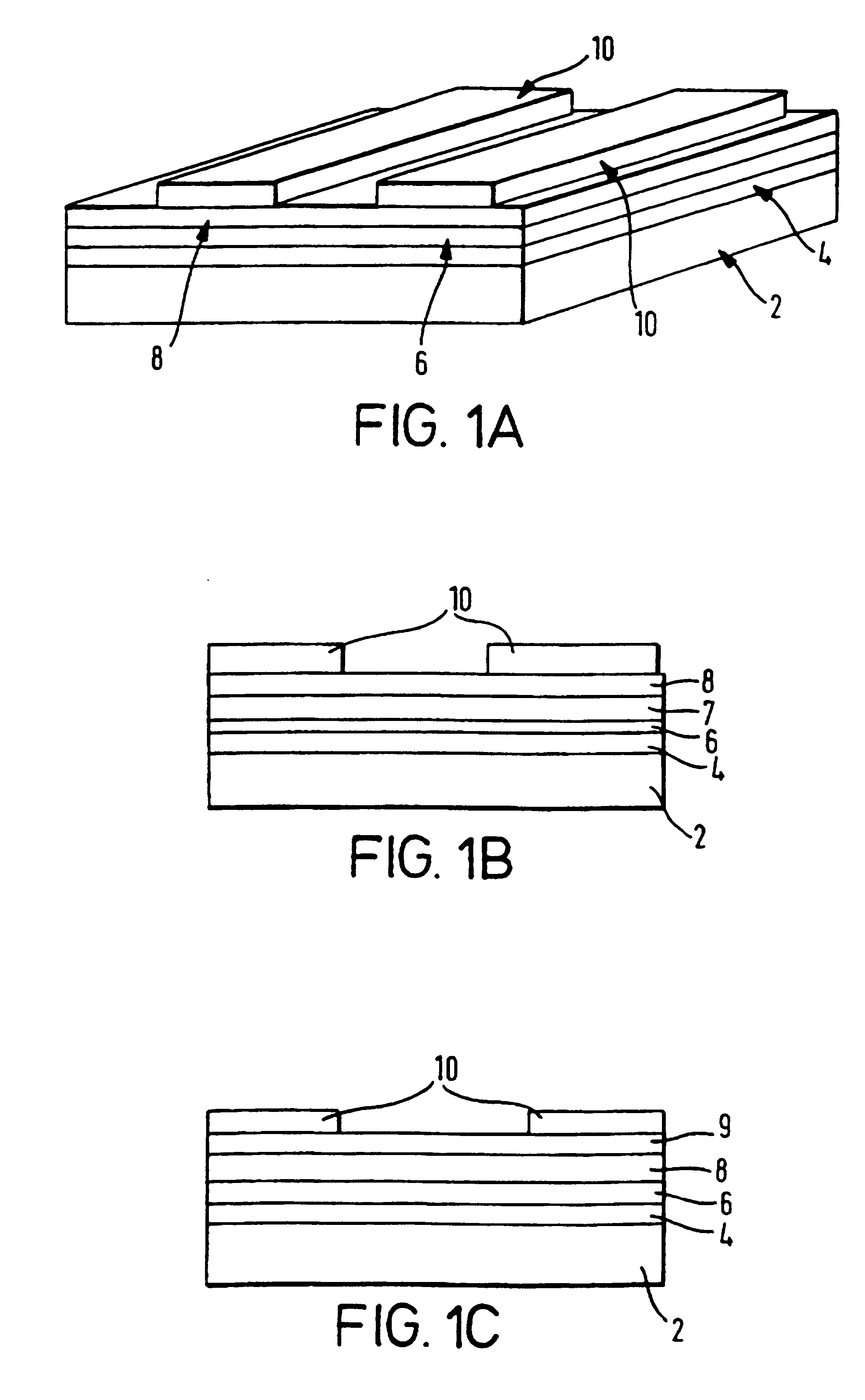
[0049] A first embodiment is now described. Indium tin oxide constituting the anode 4 is deposited using either dc or rf sputtering techniques onto the polished glass substrate 2. Such substrates are available commercially. Soda lime glass with a thin silica barrier and an indium tin oxide layer of resistivity of 30 Ohm / square and transparency of about 85%, with a thickness of order 1500 Å, can be used. A polythiophene based conducting polymer system is used as the anode protection layer 6. Polyethylene dioxythiophene / polystyrene sulphonate (PEDT / PSS @ 1:1.2 molar ratio)—which is available from Bayer AG, Leverkusen, Germany as Trial Product AI 4071. A 100 Å film of the conducting polymer is spin-coated on the substrate. The EL layer 8 is formed by spin-coating a precursor polymer such as a homopolymer PPV. With this precursor polymer the solubilising group that is removed during conversion at 150° C. in nitrogen for 4 hours is tetrahydrothiophene, and the counter-ion to the thiophen...

embodiment ii

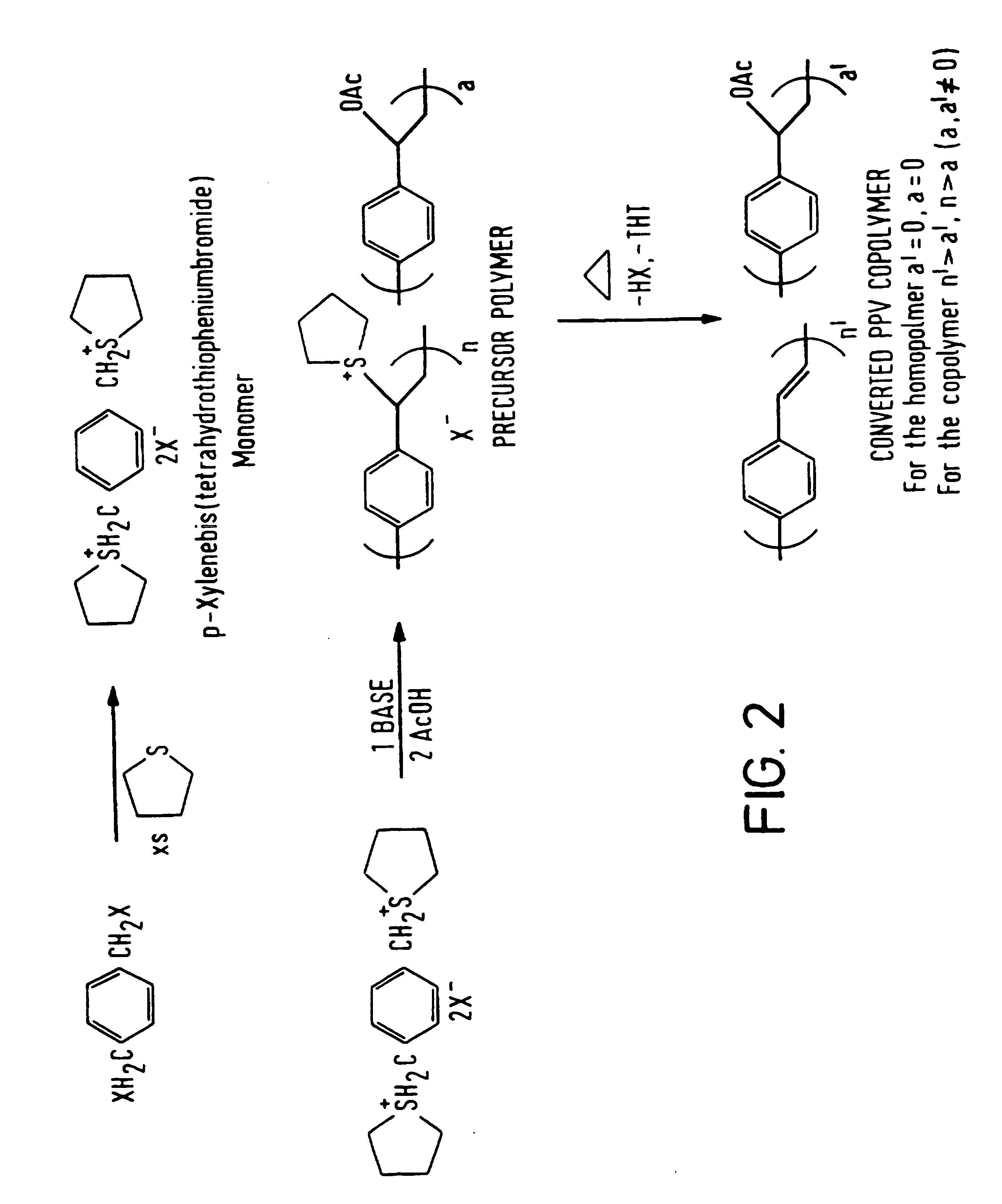
[0051] Another specific embodiment is now described. The initial steps are the same as embodiment I up to formation of the EL layer. In this embodiment, a precursor to an acetate-based PPV copolymer is deposited. This material has a very high photoluminescence (PL) efficiency, where the solubilising group that is removed during conversion is tetrahydrothiophene, and the counter-ion to the thiophene salt is bromide. Another by-product is therefore hydrogen bromide which readily attacks ITO and can cause the release of detrimental products into the film which quenches the photoluminescence and causes enhanced conversion. Without the anode protection layer 6, the PL efficiency of the PPV material is dramatically reduced from about 50-60% to, at best about 7% following the thermal conversion process (150° C. in nitrogen for 4 hours as before). However, with the protector layer a PL efficiency of ˜22% is obtained following conversion. FIG. 2 shows the conversion system, where a≠0, a≠0. A...

embodiment iii

[0055] Another specific embodiment is now described. In this embodiment, the production steps are the same for Embodiment II except that the polyethylene dioxythiophene / polystyrene sulphonate material which is used as the anode protection layer has been optimised to give beneficial lifetime performance by increasing the PSS content. Thus, the material now has a 1:5 molar ratio PEDT / PSS. The device performance of these system may be summarised as 100 cd / m2 starting brightness, efficiency of 0.3-1.2 lm / W, and up to 2 lm / W with a half-life of ˜500 hours and up to 2000 hours.


PUM

PropertyMeasurementUnit
sheet resistancesaaaaaaaaaa

Abstract

A method of manufacturing an electroluminescent device which has an anode and a cathode and arranged between the anode and the cathode a light emissive layer, also includes an anode protection layer which protects the anode against the effects of converting a precursor polymer to a semiconductive conjugated polymer which constitutes the light emissive layer. This has been found to increase the brightness and half-life of devices.

Description

FIELD OF THE INVENTION [0001] This invention relates to the construction of organic electroluminescent (EL) devices. BACKGROUND OF THE INVENTION [0002] Organic electroluminescent devices are made from materials that emit light when a suitable voltage is applied across electrodes deposited on either side of the material. One class of such materials is semiconductive conjugated polymers which have been described in our earlier U.S. Pat. No. 5,247,190, the contents of which are herein incorporated by reference. Poly (p-phenylene vinylene) [PPV], for instance, will emit light when positive and negative charge carriers are passed through the material by applying a voltage between two suitable electrodes. The electroluminescent efficiency of these devices depends on the balancing of the electrons and holes that are injected into the device and meet to form electron / hole pairs, as well as on the efficiency with which these electron / hole pairs combine to radiate light, i.e. the photolumines...

Claims


Application Information

Patent Timeline
Patent Type & Authority Applications(United States)
IPC IPC(8): H01J1/62H01J63/04C08G61/00H05B33/28C09K11/06H01L51/00H01L51/30H01L51/50H01L51/52H05B33/10H05B33/12H05B33/14
CPCC08G61/00C09K11/06H01L51/0034H01L51/0035H01L51/0036H01L51/0038H01L51/5088H01L51/5206H05B33/10H05B33/12H05B33/14Y10S428/917H10K85/10H10K85/111H10K85/114H10K85/113H10K50/17H10K50/81
Inventor PICHLER, KARLTOWNS, CARL
Owner CAMBRIDGE DISPLAY TECH LTD
Why Eureka
Try Eureka