Resist pattern thickening material and process for forming resist pattern, and semiconductor device and process for manufacturing the same

a technology of resist pattern and thickening material, which is applied in the direction of photosensitive materials, photosensitive materials auxiliaries/base layers, instruments, etc., can solve the problem of inability to thicken resist pattern without utilizing residual acid, and achieve uniform thickening effect, efficient thickening, and fine structure

Inactive Publication Date: 2006-08-24
FUJITSU LTD
View PDF13 Cites 25 Cited by
  • Summary
  • Abstract
  • Description
  • Claims
  • Application Information

AI Technical Summary

Benefits of technology

[0015] In view of the above-mentioned problems, inventors of the present invention have investigated vigorously, and have found the following experiences or discoveries. Specifically, when a resist pattern is swelled using a conventional resist swelling material, it was impossible to thicken the resist pattern without utilizing residual acid. However, they have found that when a resin, benzyl alcohol benzylamine, derivatives thereof, and the like are used as a composition of the resist patter thickening material, the reaction can be easily controlled because crosslinking reaction does not occur, and resist patterns can be thickened without depending on the sizes thereof. In addition, they have found that since the benzyl alcohol or the like has an aromatic ring at a portion of its structure, a resist pattern thickening material having high etch resistance can be obtained, and have accomplished the present invention.
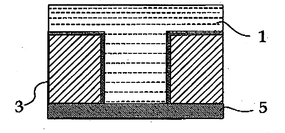
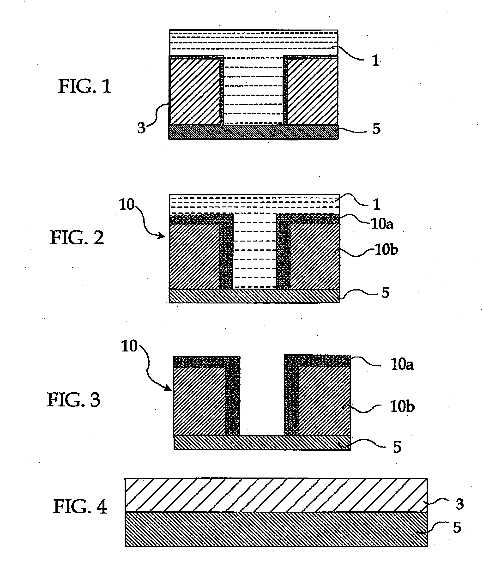
[0020] When the resist pattern thickening material is applied over a resist pattern to be thickened, the portions of the applied resist pattern thickening material in a vicinity of the interface with the resist pattern to be thickened infiltrate into the resist pattern and cause an interaction, i.e., mixing, with the material of the resist pattern to be thickened. Then, because the affinity is high between the resist pattern thickening material and the resist pattern to be thickened, a surface layer or mixing layer, where the resist pattern thickening material and the resist pattern are mixed, is efficiently formed on the surface of the resist pattern as the inner layer. As a result, the resist pattern to be thickened is efficiently thickened by the resist patter thickening material. The resist pattern thickened in this way (hereinafter sometimes referring to as “thickened resist pattern”) is thickened uniformly by the resist pattern thickening material. Thus, the space pattern of resist formed by the thickened resist pattern a fine space pattern of resist has a fine structure, exceeding exposure limits or resolution limits. The term “space pattern” is hereby defined as a hole, trench, recess, or any other empty space that is formed by developing a resist. Since the resist pattern thickening material of the present invention includes the compound represented by the general formula (1), uniform thickening effect is derived without being affected by the types of resist material or sizes of the resist pattern. Further, since the compound represented by the general formula (1) includes an aromatic ring, the resist pattern thickening material of the present invention has high etch resistance. Thus, the resist pattern thickening material of the present invention can be suitably utilized for forming a resist pattern, such as a lines and spaces pattern, on a wiring layer of LOGIC LSI where various sizes of resist patterns are utilized.
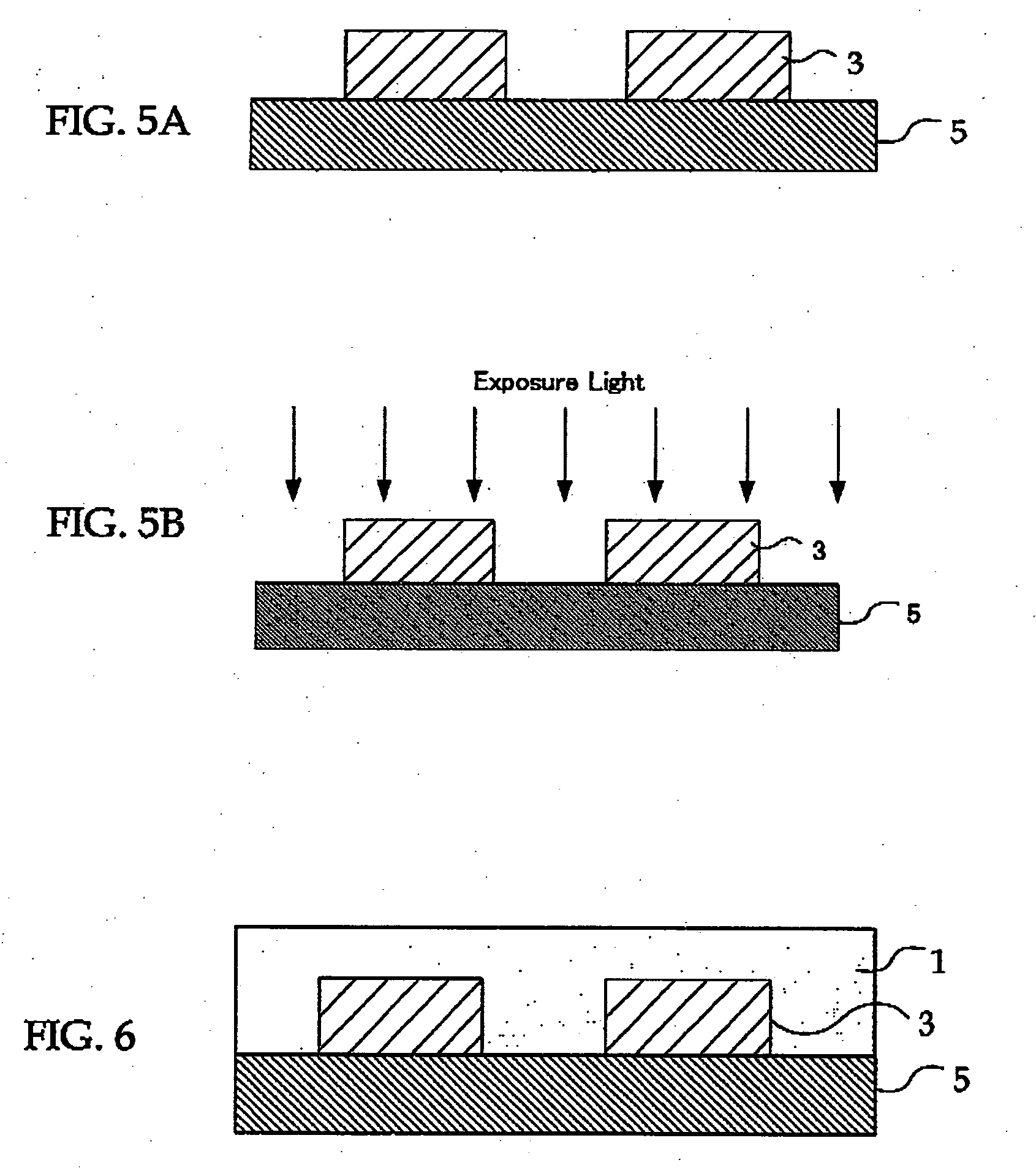
[0021] The process for forming a resist pattern of the present invention includes forming a resist pattern to be thickened, and then applying a resist pattern thickening material of the present invention so as to cover the surface of the resist pattern to be thickened. In the process for forming a resist pattern of the present invention, a resist pattern to be thickened is formed and then, when the resist pattern thickening material is applied over the resist pattern to be thickened, the portions of the applied resist pattern thickening material in a vicinity of the interface with the resist pattern to be thickened infiltrate into the resist pattern and cause an interaction or mixing with the material of the resist pattern. Thus, a surface layer or fig layer, where the resist pattern thickening material and the resist pattern are mixed, is formed on the surface of the resist pattern as the inner layer. The resulting thickened resist patter is uniformly thickened by the resist pattern thickening material. Thus, the space pattern of resist formed by the thickened resist pattern a fine space pattern of resist has a fine structure, exceeding exposure limits or resolution limits. Since the resist pattern thickening material includes the compound represented by the general formula (1), uniform thickening effect is derived without being affected by the types of resist material or sizes of the resist pattern. Further, the aromatic ring in the compound represented by the general formula (1) provides high etch resistance. Thus, the process for forming a resist pattern can be suitably utilized for forming a resist pattern, such as a line-space pattern, on a wiring layer of LOGIC LSI where not only a contact hole pattern, but also various sizes of resist patterns are utilized.
[0022] The process for manufacturing a semiconductor device of the present invention includes a step of forming a thickened resist pattern on a surface of a workpiece using the process for forming a resist pattern of the present invention, namely, a step of forming a thickened resist pattern by forming a resist pattern to be thickened on a surface of a workpiece, and then by applying a resist pattern thickening material so as to cover the surface of the resist pattern to be thickened; and a step of pattering the surface of the workpiece by etching the surface of the workpiece using the thickened resist pattern as a mask. In the process for manufacturing a semiconductor device, initially, in the step of forming a thickened resist patter, a resist pattern to be thickened is formed on the surface of the workpiece serving as a subject on which wiring patterns, etc. is formed, and then the resist pattern thickening material of the present invention is applied so as to cover the surface of the resist pattern to be thickened. Then, the portions of the applied resist pattern thickening material in a vicinity of the interface with the resist pattern to be thickened infiltrate into the resist pattern and cause an interaction or mixing with the material of the resist pattern. Thus, a surface layer or mixing layer, where the resist pattern thickening material and the resist pattern are mixed, is formed on the surface of the resist pattern as the inner layer. The resulting thickened resist pattern is uniformly thickened by the resist pattern thickening material. Thus, the space patter of resist formed by the thickened resist pattern has a fine structure, exceeding exposure limits or resolution limits. Since the resist patter thickening material includes the compound represented by the general formula (1), uniform thickening effect is derived without being affected by the types of resist material or sizes of the resist pattern. Further, the aromatic ring in the compound represented by the general formula (1) provides high etch resistance. Thus, thickened resist patterns such as a line-space pattern, on a wiring layer of LOGIC LSI where not only a contact hole pattern, but also various sizes of resist patterns are utilized, can be formed easily and precisely.
[0023] In the step of patterning, by etching the surface of the workpiece using the thickened resist pattern formed by the step of forming a thickened resist pattern as a mask the surface of the workpiece is patterned finely and precisely with accurate dimension, thus high-quality and high performance semiconductor devices can be produced efficiently having a wiring pain with fine, precise, and accurate dimension.
[0024] The semiconductor device of the present invention is manufactured by the process for manufacturing a semiconductor device of the present invention. The semiconductor device has patterns, for example, wiring patterns, with fine, precise, and accurate dimension, and is high quality and high performance.

Problems solved by technology

Specifically, when a resist pattern is swelled using a conventional resist swelling material, it was impossible to thicken the resist pattern without utilizing residual acid.

Method used


Image

  • Resist pattern thickening material and process for forming resist pattern, and semiconductor device and process for manufacturing the same
  • Resist pattern thickening material and process for forming resist pattern, and semiconductor device and process for manufacturing the same
  • Resist pattern thickening material and process for forming resist pattern, and semiconductor device and process for manufacturing the same

Examples


example 1

Preparation of Resist Pattern Thickening Material

[0237] Resist pattern thickening materials A through T having the compositions shown in Table 1 were prepared.

[0238] Note that, in Table 1, the “thickening material” means a resist pattern thickening material, and “A” through “T” correspond to the resist pattern thickening materials A through T. Of the resist pattern thickening materials A through T, the resist pattern thickening materials A, B, and P correspond to comparative example and the resist pattern thickening materials C to O and Q to T correspond to examples (of the present invention). Note that, in Table 1, the unit of the values in parentheses is parts by mass.

[0239] In the “compound represented by the general formula (1)” column of resist pattern thickening materials C to O and Q to T, benzyl alcohol, benzylamine, and a derivative thereof are compounds represented by the following general formula (1).

[0240] In the general formula (1), “X” is a functional group repre...

example 2

Preparation of Resist Pattern Thickening Material

[0262] Resist pattern thickening materials 2A through 2D having the composition shown in Table 7 were prepared.

[0263] In Table 7, “thickening material” means a resist pattern thickening material, and “2A” through “2D” correspond to the resist pattern thickening materials 2A through 2D. In Table 7, the unit of the values in parentheses is parts by mass.

[0264] In the “compound represented by general formula (1)” column of the resist pattern thickening materials 2A through 2D, derivatives of benzyl alcohol are compounds represented by the above-mentioned general formula (1).

[0265] In the “resin” column, “PVA” is a polyvinyl alcohol resin (“PVA-205C” manufactured by Kuraray Co., Ltd.). In the “surfactant” column, “TN-80” is a non-ionic surfactant (a primary alcohol ethoxylate surfactant manufactured by Asahi Denka Co., Ltd.), and “PC-6” is a non-ionic surfactant (a polynuclear phenol ethoxylate surfactant manufactured by Asahi Denka ...

example 3

Preparation of Resist Pattern Thickening Material

[0273] Resist pattern thickening materials 3A through 3E having the compositions shown in Table 10 were prepared.

[0274] Note that, in Table 10, the thickening material” means a resist pattern thickening material, and “3A” through “3E” correspond to the resist pattern thickening materials 3A through 3E. Note that, in Table 10, the unit of the values in parentheses is parts by mass.

[0275] In the “compound represented by the general formula (1)” column of the resist pattern thickening materials 3A through 3E, derivatives of benzyl alcohol are compounds represented by the above-mentioned general formula (1).

[0276] In the “resin” columns “PVA” is a polyvinyl alcohol resin (“PVA-205C” manufactured by Kuraray Co., Ltd.) and “KW-3” is a polyvinyl acetal resin (manufactured by Sekisui Chemical Co., Ltd.). In the “surfactant” column, “PC-6” is a non-ionic surfactant (a polynuclear phenol ethoxylate surfactant manufactured by Asahi Denka Co...


PUM

PropertyMeasurementUnit
wavelengthaaaaaaaaaa
temperatureaaaaaaaaaa

Abstract

The present invention provides a resist pattern thickening material, which can utilize ArF excimer laser light; which, when applied over a resist pattern to be thickened e.g., in form of lines and spaces pattern, can thicken the resist pattern to be thickened regardless of the size of the resist pattern to be thickened; and which is suited for forming a fine space pattern or the like, exceeding exposure limits. The present invention also provides a process for forming a resist pattern and a process for manufacturing a semiconductor device, wherein the resist pattern thickening material of the present invention is suitably utilized.

Description

CROSS-REFERENCE TO RELATED APPLICATIONS [0001] This application is based upon and claims the benefits of the priority from the prior Japanese Patent Application No. 2005-042884 filed on Feb. 18, 2005 and Japanese Patent Application No. 2005-366991, filed on Dec. 20, 2005, the entire contents of which are incorporated herein by reference. BACKGROUND OF THE INVENTION [0002] 1. Field of the Invention [0003] The present invention relates to a resist pattern thickening material, which is applied over a resist pattern that is formed in manufacturing a semiconductor device and is capable of thickening the resist pattern, and which may form a fine space pattern that exceeds exposure limits of light sources of available exposure devices. The present invention also relates to a process for forming a resist pattern, a semiconductor device, and a process for manufacturing the semiconductor device that utilize the resist pattern thickening material respectively. [0004] 2. Description of the Rela...

Claims


Application Information

Patent Timeline
Patent Type & Authority Applications(United States)
IPC IPC(8): G03C1/76
CPCG03F7/2024G03F7/40G11B5/3163H01L21/0274H01L21/0275H01L27/115H01L27/11526H01L27/11543Y10S430/106Y10S430/114H10B41/48H10B41/40H10B69/00G03F7/11
Inventor NOZAKI, KOJIKOZAWA, MIWANARRIKI, TAKAHISA
Owner FUJITSU LTD
Why Eureka
Try Eureka