Manufacturing Method of Semiconductor Device

a manufacturing method and semiconductor technology, applied in the field of semiconductor devices, can solve the problems of increased size, heavy and easily broken, glass substrates and quartz substrates are not suitable for mass production, etc., and achieve the effects of reducing weight, short time, and smooth peeling

Inactive Publication Date: 2006-09-07
SEMICON ENERGY LAB CO LTD
View PDF27 Cites 52 Cited by
  • Summary
  • Abstract
  • Description
  • Claims
  • Application Information

AI Technical Summary

Benefits of technology

[0026] In addition, by a manufacturing method of the invention, a thin film integrated circuit including a TFT can be peeled off from a glass substrate and further transferred to a flexible substrate. By transferring the thin film integrated circuit including a TFT to the flexible substrate, mass production can be realized, in which many thin film integrated circuits are formed over one substrate. Further, by transferring a thin film integrated circuit to a flexible substrate, a semiconductor device itself, on which the thin film integrated circuit is mounted, can be reduced in weight.
[0027] According to the invention, by utilizing both a physical force and a chemical reaction, peeling can be smoothly performed in a short time.

Problems solved by technology

A glass substrate or a quartz substrate is currently used in many cases; however, there is a problem in that it is heavy and easily broken.
In addition, a glass substrate and a quartz substrate are not suitable for mass production since they have a difficulty of being increased in size.
However, since the plastic film has low heat resistance, maximum process temperature is required to be low.
As a result, a TFT having more favorable electric characteristics than that in the case of forming a TFT over a glass substrate cannot be formed in the present situation.

Method used


Image

  • Manufacturing Method of Semiconductor Device
  • Manufacturing Method of Semiconductor Device
  • Manufacturing Method of Semiconductor Device

Examples


embodiment mode 1

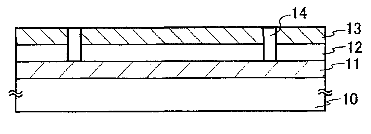
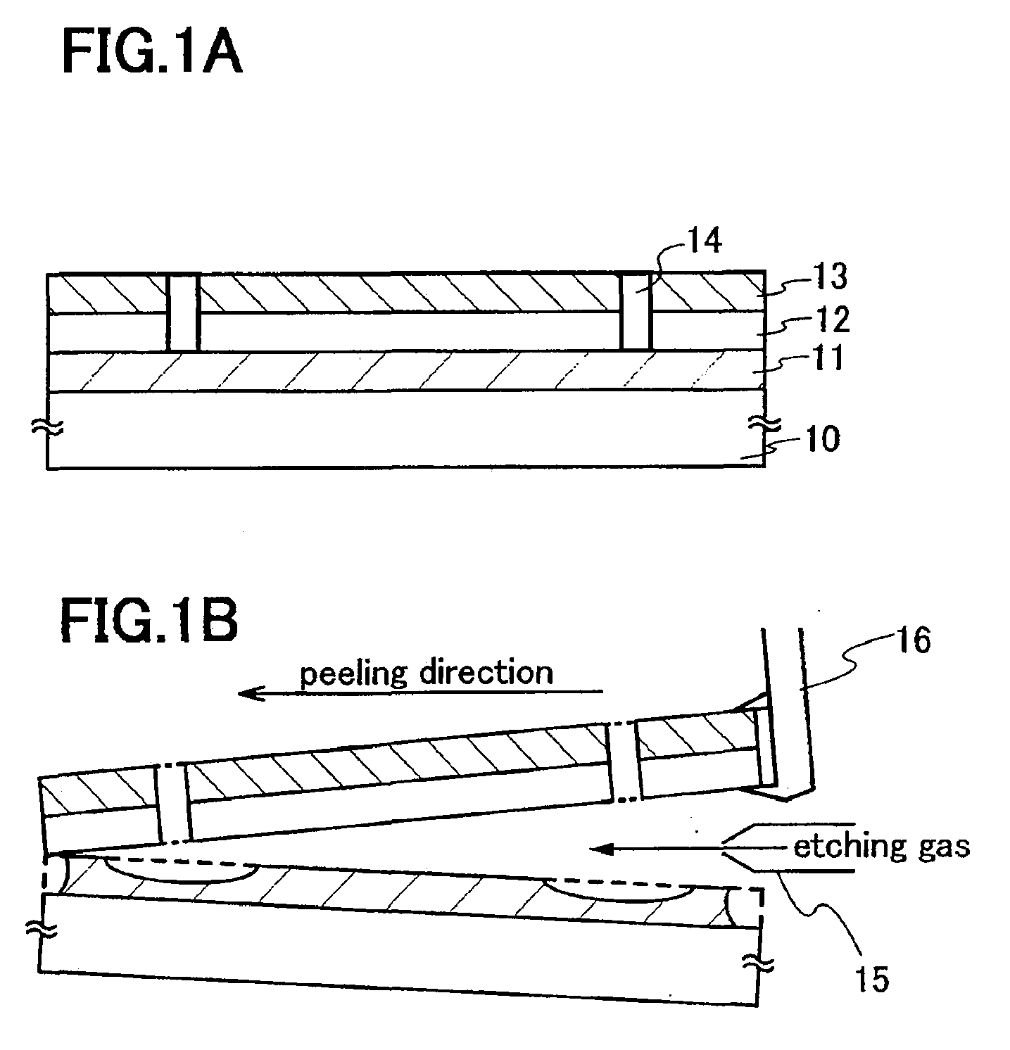
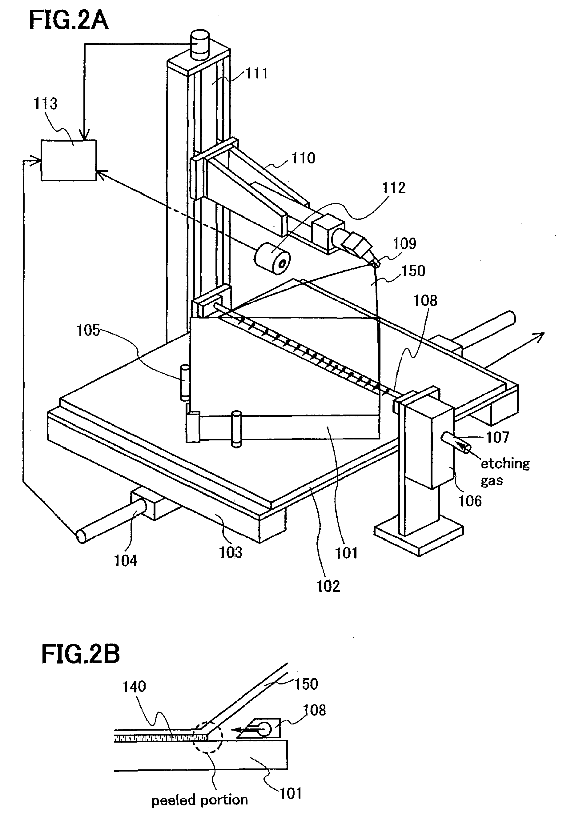
[0037] In Embodiment Mode 1, a manufacturing method is described, in which a layer to be peeled including a TFT formed over a glass substrate is peeled off from the glass substrate and then transferred onto a plastic substrate. Here, an example of removing a layer to be peeled with a halogen gas blowing to a peeling layer in an atmosphere containing a halogen gas is described.

[0038] First, a peeling layer 11 is formed on a glass substrate 10. As the peeling layer 11, a single layer or a laminated layer formed of an element selected from W, Ti, Ta, Mo, Cr, Nd, Fe, Ni, Co, Zr, Zn, Ru, Rh, Pd, Os, or Ir, or an alloy material or a compound material containing the element as its main component can be used. Alternatively, a single layer or a laminated layer formed of nitride of the above-described element such as titanium nitride, tungsten nitride, tantalum nitride, or molybdenum nitride can be used. The thickness of the peeling layer 11 is 10 nm to 200 nm, preferably 50 nm to 75 nm.

[00...

embodiment mode 2

[0069] Though an example of performing the peeling in a halogen gas atmosphere is described in Embodiment Mode 1, an example of performing peeling in an etchant will be described here.

[0070] Similarly to Embodiment Mode 1, a peeling layer 21 is formed over a glass substrate 20, and an insulating film and a layer to be peeled 22 including a plurality of TFTs, which is provided over the insulating film, are formed. In this embodiment mode, a silicon film is used as the peeling layer 21. A protective layer 23 is formed in the same manner as in Embodiment Mode 1. The protective layer 23 is formed using a material which does not react with an etchant to be used in a subsequent step, for example, an organic resin.

[0071] Subsequently, dry etching or wet etching is performed using a mask. In this etching step, an opening portion 24 reaching the peeling layer 21 is selectively formed in a region except a region provided with the TFT, a wiring, or the like, so as to expose the peeling layer...

embodiment 1

[0083] In Embodiment 1, a case of using a thin film integrated circuit as an IC chip will be described.

[0084] The IC chip can be roughly divided into three types: a contactless type IC chip mounted with an antenna (also referred to as a wireless tag), a contact type IC chip provided with a terminal connected to an external power source without a mounted antenna, and a hybrid type IC chip which is a combination of the contactless type and the contact type.

[0085] In the case of using the thin film integrated circuit as the contact type IC chip, the thin film integrated circuit peeled by a peeling method of the present invention can be used by being directly mounted on an article.

[0086] On the other hand, in the case of using the thin film integrated circuit as the contactless type IC chip or the hybrid type IC chip, the integrated circuit is preferably used with a mounted antenna. Examples of a cross-sectional view of the IC chip, on which an antenna is mounted, are shown in FIGS. ...


PUM


Abstract

The present invention has an object to perform a peeling treatment in a short time. Peeling is performed while a peeling layer is exposed to an atmosphere of an etching gas. Alternatively, peeling is performed while an etching gas for a peeling layer is blown to the peeling layer in an atmosphere of an etching gas. Specifically, an etching gas is blown to a part to be peeled while a layer to be peeled is torn off from a substrate. Alternatively, peeling is performed in an etchant for a peeling layer while supplying an etchant to the peeling layer.

Description

BACKGROUND OF THE INVENTION [0001] 1. Field of the Invention [0002] The present invention relates to a semiconductor device having a circuit including a thin film transistor (hereinafter referred to as a TFT) and a manufacturing method thereof. For example, the invention relates to an electro-optical device typified by a liquid crystal display device having a liquid crystal display panel, a light emitting display panel including an organic light emitting element, or an electronic device on which an integrated circuit having an antenna is mounted as a part. [0003] In this specification, a semiconductor device refers to all types of devices which can function by using semiconductor characteristics. An electro-optical device, a semiconductor circuit, and an electronic device are included in the category of all semiconductor devices. [0004] 2. Description of the Related Art [0005] Recently, a technique of making a thin film transistor (TFT) using a semiconductor thin film (approximately...

Claims


Application Information

Patent Timeline
Patent Type & Authority Applications(United States)
IPC IPC(8): H01L21/44H01L21/461
CPCH01L21/67132H01L27/1266H01L27/1214H01L21/7806H01L21/31111H01L21/6708H01L2021/775
Inventor SUGIYAMA, EIJIDOZEN, YOSHITAKAFUKUMOTO, YUMIKOKUWABARA, HIDEAKIYAMAZAKI, SHUNPEI
Owner SEMICON ENERGY LAB CO LTD
Why Eureka
Try Eureka