Semiconductor device and a method of manufacturing the same and designing the same

a technology of semiconductor devices and dummy structures, applied in semiconductor devices, semiconductor/solid-state device details, electrical apparatus, etc., can solve the problems of complex shape of dummy structures and imperfect insulation films, and achieve the effect of improving the flatness of the surface of the insulation film embedded in the isolation groove, increasing the number of dummy patterns, and increasing the amount of coordinate data

Inactive Publication Date: 2006-09-14
RENESAS ELECTRONICS CORP
View PDF12 Cites 5 Cited by
  • Summary
  • Abstract
  • Description
  • Claims
  • Application Information

AI Technical Summary

Benefits of technology

[0015] In the second dummy pattern placing method, since the size of the dummy patterns DPA2 is relatively small, the dummy patterns DPA2 may be placed up to the area near the boundary BL between the element forming region DA and dummy region FA. Thereby, since the dummy patterns DPA2 may be placed also in the region where the dummy patterns DPA1 cannot be placed, the second dummy pattern placing method can further improve the flatness of the surface of the embedded insulation film up to the dummy region FA near the boundary BL in comparison with the first dummy pattern placing method.
[0016] However, when the second dummy pattern placing method is introduced, the number of dummy patterns DPA2 placed in the dummy region FA increases, and, thereby, the coordinate data required for generating a mask remarkably increases. As a result, there arises a problem in that the arithmetic processing time in computer used for generating a mask pattern increases, and, moreover, the time required for drawing the patterns on the mask substrate also increases, with the result that the throughput in the formation of a mask is remarkably deteriorated. Particularly, when the second dummy pattern placing method is employed for ASIC (Application Specific Integrated Circuit: integrated circuit for particular application), the time required to generate the mask is extended, with the result that a problem remains for development of ASIC within a short period of time.
[0017] It is therefore an object of the present invention to provide a technique to improve the flatness of the surface of members embedded in a plurality of recesses.
[0018] It is another object of the present invention to provide a technique to improve the flatness of the surface of members embedded in a plurality of recesses without extension of the time required for manufacturing the semiconductor device.
[0024] According to the features explained above, a plurality of dummy patterns can be placed up to the area near the boundary between the element forming region and dummy region. Thereby, the flatness of the surface of the insulation film embedded in the isolation grooves can be improved over the entire area of the dummy region.
[0025] Moreover, since a relatively wide region in the dummy region can be occupied by a plurality of dummy patterns of relatively wider area, while the remaining relatively narrow region can be occupied with a plurality of dummy patterns of relatively narrow area, an increase in the number of dummy patterns can be controlled. Therefore, an increase in the amount of coordinate data which needs to be produced at the time of generating a mask can also be controlled with a view toward controlling an increase in the arithmetic processing time of a computer used for such processing and the time for drawing a pattern on the mask substrate.

Problems solved by technology

However, according to an investigation by the inventors of the present invention, there has been a further problem in that, when the dummy structures are placed in the non-active device area, some dummy structures are complicated in shape and the insulation film is not perfectly embedded within the internal side of the dummy structures which are particularly defined.

Method used


Image

  • Semiconductor device and a method of manufacturing the same and designing the same
  • Semiconductor device and a method of manufacturing the same and designing the same
  • Semiconductor device and a method of manufacturing the same and designing the same

Examples


embodiment 1

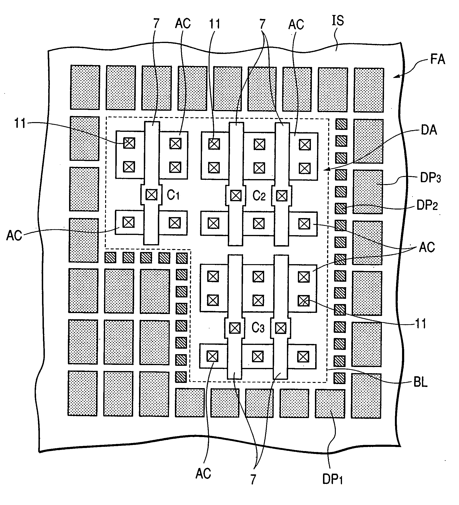
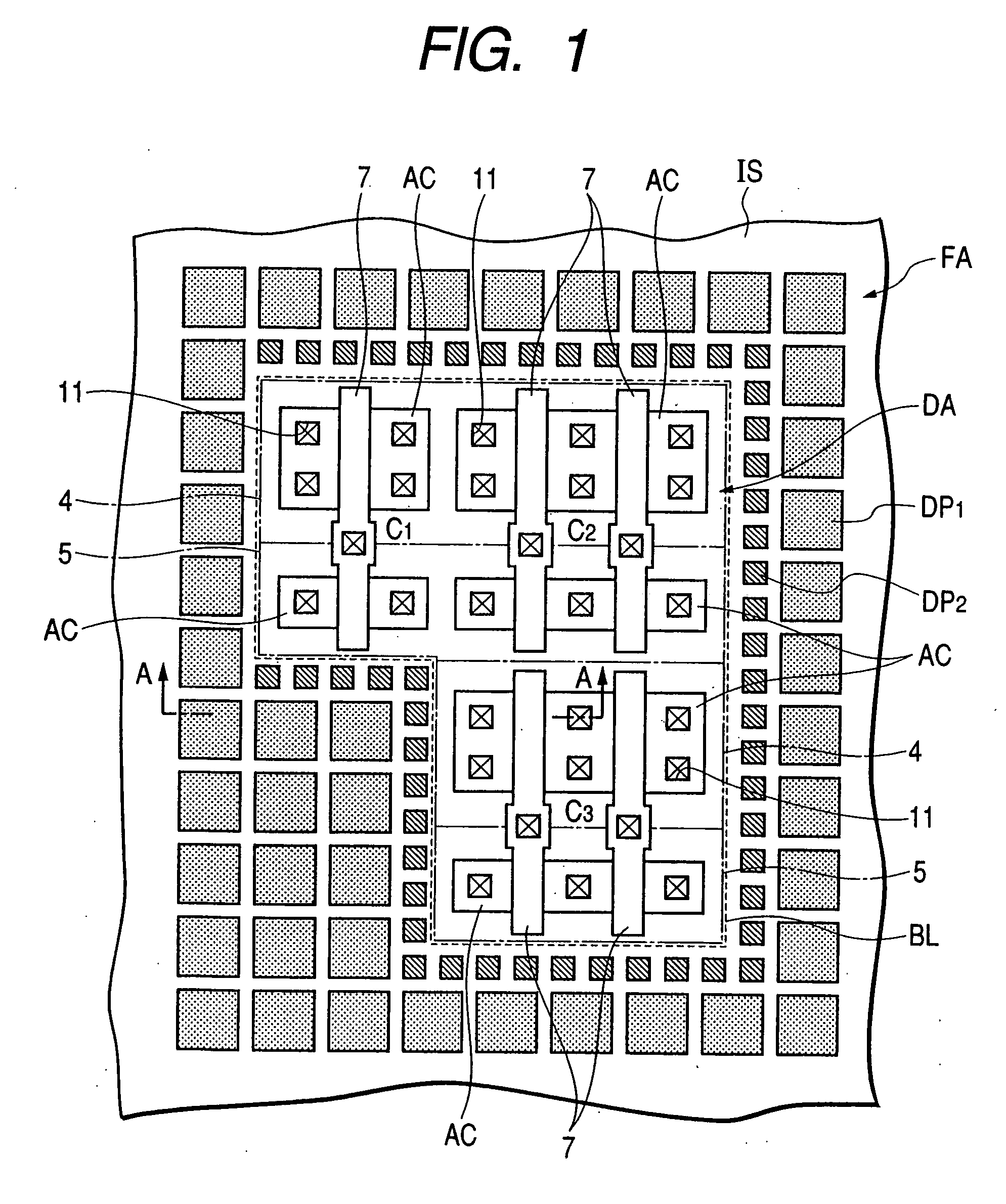
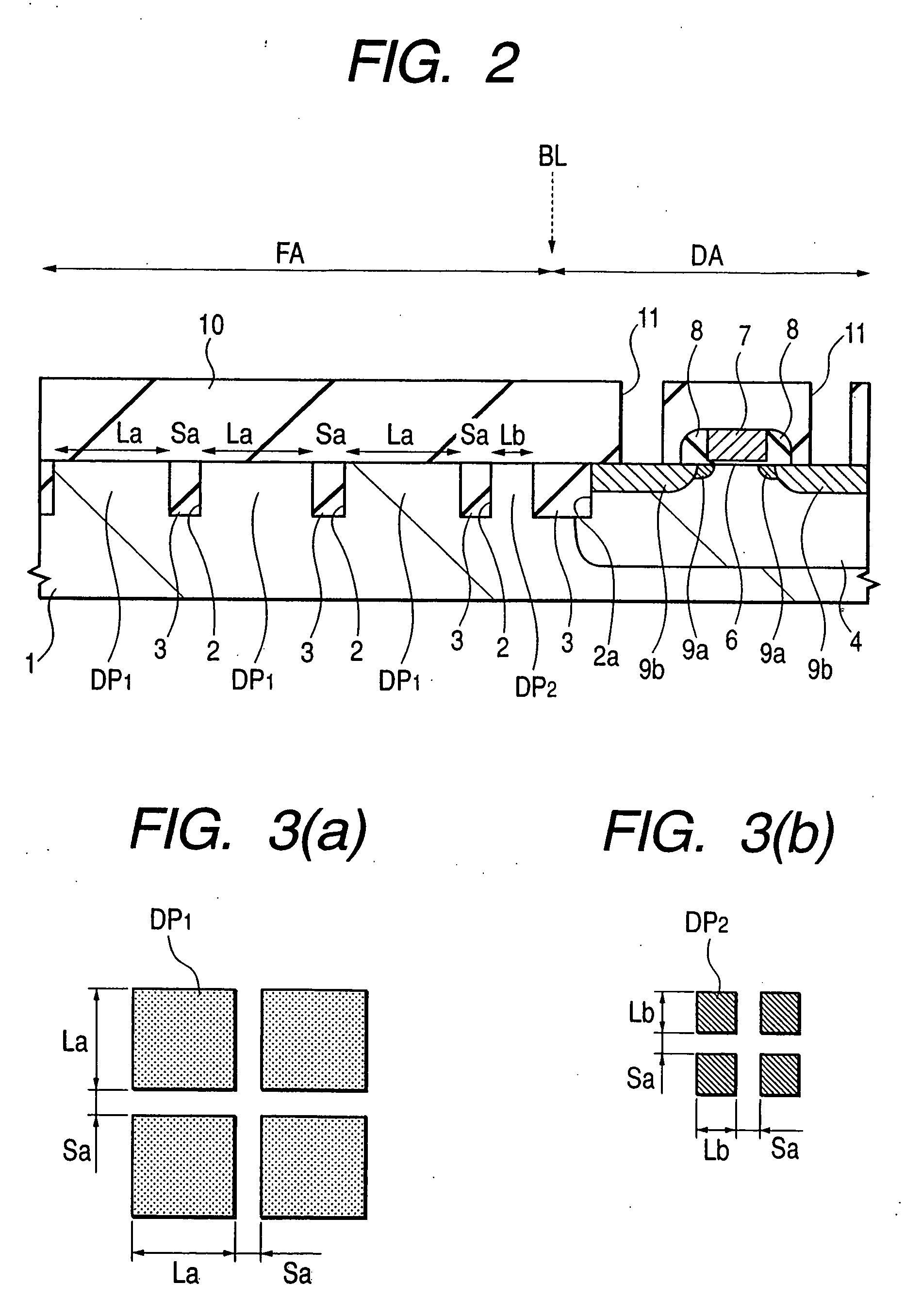
[0057] An example of the placement of dummy patterns according to embodiment 1 of the present invention will be explained with reference to FIG. 1 to FIG. 5. FIG. 1 is a plan view of an example of a logic integrated circuit device. FIG. 2 is a cross-sectional view taken along the line A-A of FIG. 1. FIGS. 3(a) and 3(b) are plan views showing a pitch and a size of the dummy patterns. FIG. 4 is a plan view showing an example of the placement of the dummy patterns. FIG. 5 is a process flow diagram showing an example of a method of generating the dummy patterns.

[0058] As shown in FIG. 1, the area inside of the boundary BL, which is indicated by a broken line, represents the element forming region DA where semiconductor elements are formed, while the area outside of the boundary BL represents the dummy region FA where semiconductor elements are not formed.

[0059] The boundary BL between the element forming region DA and dummy region FA is determined from a layout of the conductive film ...

embodiment 2

[0090] The embodiment 2 of the present invention is directed to another manufacturing method that can be used to form the structure of FIG. 1.

[0091]FIG. 17 and FIG. 18, which illustrate the embodiment 2, are cross-sectional views of a portion of a semiconductor substrate after completion of the manufacturing processes explained with reference to FIGS. 6 and 7.

[0092] In this embodiment, the isolation grooves 2, 2a are formed first to a depth of about 0.3 to 0.4 μm on the semiconductor substrate 1, and then the silicon oxide film 3 is deposited on the semiconductor substrate 1 using the CVD method or plasma CVD method.

[0093] Next, as shown in FIG. 17, a coated insulation film 18, for example, an SOG (Spin On Glass) film, is formed as the upper layer of the silicon oxide film 3. This coated insulation film 18 can be flattened at its surface even when a fine level-difference exists due to the fluidity of the film. Therefore, even if a recess is generated at the surface of the silicon...

embodiment 3

[0097] The embodiment 3 is directed to another manufacturing method that can be used to form the structure of FIG. 1, and this embodiment will be explained with reference to FIG. 19 to FIG. 22.

[0098] First, as shown in FIG. 19, a semiconductor substrate 1, consisting, for example, of a p-type single crystal silicon, is subjected to the thermal oxidation to form on the surface thereof a gate insulation film 19 consisting of a thin silicon oxide film having a thickness of about 2 to 3 nm. Next, a first silicon film 20 having a thickness of about 50 nm and a silicon nitride film having a thickness of about 120 to 200 nm are deposited sequentially as upper layers using the CVD method. Thereafter, the silicon nitride film 21, first silicon film 20 and gate insulation film 19 are sequentially dry-etched using a resist pattern as a mask. The first silicon film 20 is composed of a non-crystal silicon or polycrystalline silicon. Subsequently, after the resist pattern is removed, the isolati...


PUM


Abstract

There is provided a technique for improving the flatness at the surface of members embedded in a plurality of recesses without resulting in an increase in the time required for the manufacturing processes. According to this technique, the dummy patterns can be placed up to the area near the boundary BL between the element forming region DA and dummy region FA by placing the first dummy pattern DP1 of relatively wider area and the second dummy pattern DP2 of relatively small area in the dummy region FA. Thereby, the flatness of the surface of the silicon oxide film embedded within the isolation groove can be improved over the entire part of the dummy region FA. Moreover, an increase of the mask data can be controlled when the first dummy patterns DP1 occupy a relatively wide region among the dummy region FA.

Description

[0001] This application is a continuation of U.S. application Ser. No. 10 / 748,139, filed Dec. 31, 2003 which, in turn, is a divisional of U.S. application Ser. No. 09 / 985,309, filed Nov. 2, 2001, now U.S. Pat. No. 6,693,315; and the entire disclosures of which are incorporated herein by reference.BACKGROUND OF THE INVENTION [0002] The present invention relates to a semiconductor device and to a method of manufacturing the sane; and, more particularly, the invention relates to a technique that can effectively be applied to the manufacture of a semiconductor device, including a flattening process utilizing a CMP (Chemical Mechanical Polishing) method. [0003] Trench isolation is one of the isolation methods employed for electrically isolating adjacent semiconductor elements. In a typical trench isolation fabrication process, grooves are provided on a semiconductor substrate, which grooves become an element isolation region, and these grooves are filled with insulation films. [0004] Tre...

Claims


Application Information

Patent Timeline
Patent Type & Authority Applications(United States)
IPC IPC(8): H01L31/00H01L29/94H01L29/00H01L29/76H01L21/76H01L21/301H01L21/304H01L21/3105H01L21/3205H01L21/762H01L23/52H01L23/528H01L27/02H01L27/04H01L27/08H01L27/118
CPCH01L21/31053H01L21/76229H01L23/522H01L23/528H01L27/0207H01L27/11807H01L2924/0002H01L29/0649H01L21/74H01L21/76224H01L2924/00H01L27/04H01L23/5283H01L23/53228H01L29/0653H01L29/0692H01L29/4925
Inventor KURODA, KENICHIWATANABE, KOZOYAMAMOTO, HIROHIKO
Owner RENESAS ELECTRONICS CORP
Why Eureka
Try Eureka