Film or layer of semiconducting material, and process for producing the film or layer

a technology of semiconducting material and film or layer, which is applied in the direction of basic electric elements, electrical equipment, semiconductor devices, etc., can solve the problems of large number of defects, large rough surface, and adverse effects of damage on soi wafers, and achieve the effect of reducing the thickness of the silicon layer

Inactive Publication Date: 2006-09-14
SILTRONIC AG
View PDF12 Cites 4 Cited by
  • Summary
  • Abstract
  • Description
  • Claims
  • Application Information

AI Technical Summary

Benefits of technology

[0013] Therefore, complex further treatment steps are carried out in order to compensate for the above drawbacks. For example, according to EP 905767, the defect layer which has been produced by the cleaving of the silicon wafer along the layer of hydrogen bubbles, is removed from the SOI wafer by means of a vapor-phase etching process. This process at the same time allows the thickness ...

Problems solved by technology

However, the implantation of the oxygen ions produces crystal defects (damage) in the thin layer of silicon, and this damage has adverse effects on the SOI wafer during subsequent fabrication of electronic components.
The result is a relatively rough surface with a large number of defects, which then has to be smoothed by polishing or heat treatment (annealing).
Furthermore, the implantation, the sep...

Method used


Image

  • Film or layer of semiconducting material, and process for producing the film or layer
  • Film or layer of semiconducting material, and process for producing the film or layer
  • Film or layer of semiconducting material, and process for producing the film or layer

Examples


example

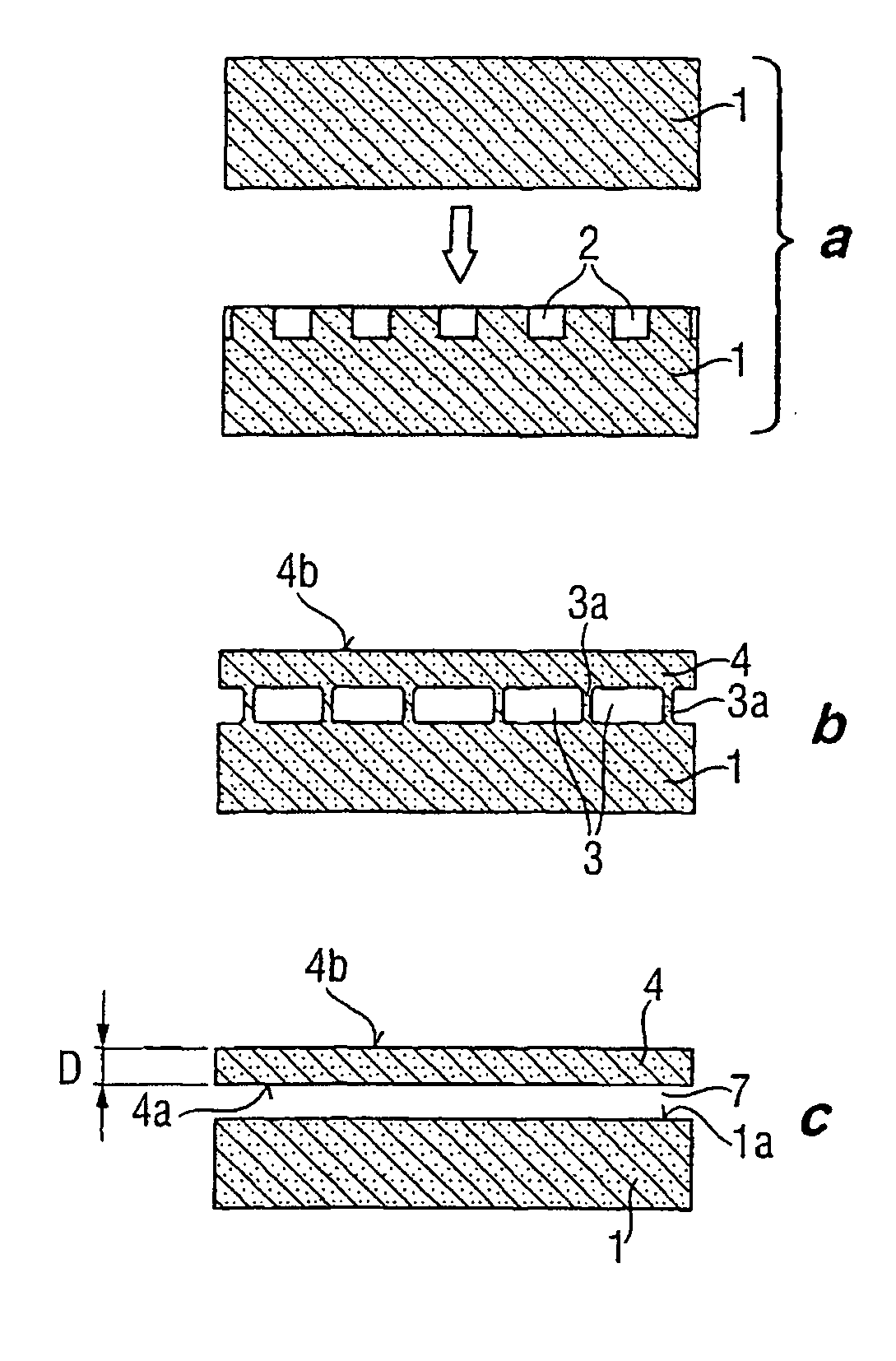
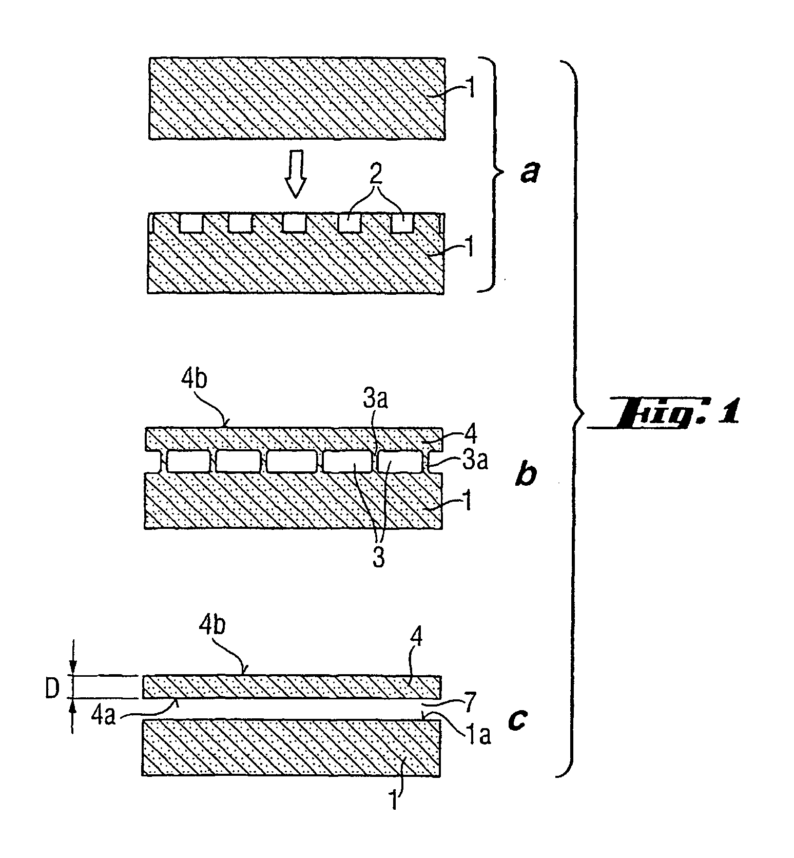
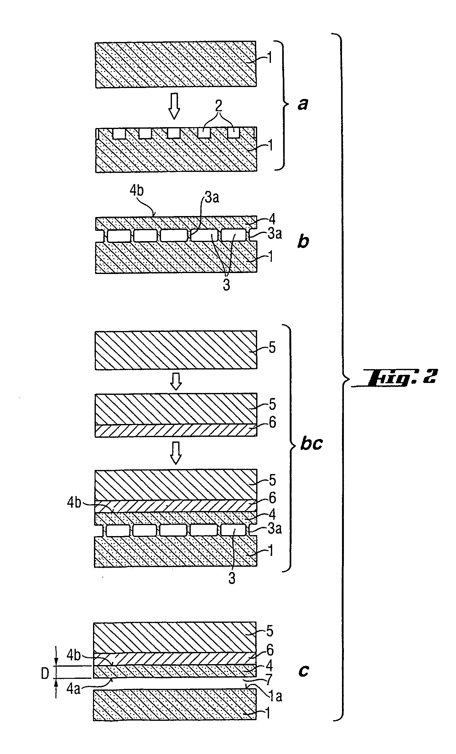
[0066] The smooth, planar surface of a silicon wafer 1 (FIG. 2) was provided with periodically recurring recesses (trenches) 2 in step a) of the process according to the invention. The trenches had a square cross section with an edge length of approx. 0.5 μm, and the trench-to-trench distance was approx. 0.9 μm. The trenches were arranged in a regular, square pattern. The trenches were produced by ion beam etching in accordance with the prior art, in such a manner that a trench depth of 3 μm resulted.

[0067] Then, the structured surface of the silicon wafer 1 was in step b) closed up by means of a heat treatment which lasts for 10 minutes in a pure hydrogen atmosphere under a pressure of 10 torr, and with a hydrogen flow rate of 10 sccm and a temperature of 1100° C. In the process, the cavities 3 formed from the trenches 2 were widened by approx. 0.25 μm parallel to the closed surface 4 of the wafer. FIG. 3 shows an SEM image of the cavities 3 which have formed and of the closed, pe...


PUM


Abstract

SOI wafers are manufactured to have very thin device layers of high surface quality. The layer is ≦ 20 nm in thickness, has an HF density of ≦ 0.1/cm2, and a surface roughness of 0.2 nm RMS.

Description

CROSS-REFERENCE TO RELATED APPLICATION [0001] This application is a division of and claims priority to U.S. application Ser. No. 10 / 481,537 filed Dec. 18, 2003, a National Stage of PCT / EP02 / 07125 filed Jun. 27, 2002, and also claims priority to German application DE 101 31 249.0 filed Jun. 28, 2001.BACKGROUND OF THE INVENTION [0002] 1. Field of the Invention [0003] The invention relates to a film or layer of semi-conducting material and to a process for producing the film or layer. [0004] 2. Description of the Related Art [0005] What are known as SOI (silicon on insulator) wafers have a layer structure generally comprising a carrier, for example a silicon wafer, a layer of oxide which is buried just below the surface and a thin layer of silicon on top of the layer of oxide. For the fabrication of electronic components (e.g. memories and microprocessors), this layer structure has significant advantages over the silicon wafers which are customarily used: [0006] A better characteristic...

Claims


Application Information

Patent Timeline
IPC IPC(8): H01L29/06H01L21/02H01L21/762H01L27/12
CPCH01L21/3223H01L21/76251H10B99/00
Inventor MURPHY, BRIANWAHLICH, REINHOLDSCHMOLKE, RUDIGERVON AMMON, WILFRIEDMORELAND, JAMES
Owner SILTRONIC AG
Why Eureka
Try Eureka