Imaging module and method for forming the same

a multi-level imaging and module technology, applied in the field of multi-level imaging modules, can solve the problems of difficult to make the optical axis, difficult to place a printed circuit board on which an imaging module and other devices can be placed, and difficult to make the center of an imaging region of an imaging semiconductor chip accurately coincide with the optical axis. , to achieve the effect of high-reliable imaging modules, easy fabrication, and convenient mounting

Inactive Publication Date: 2006-09-14
COLLABO INNOVATIONS INC
View PDF6 Cites 44 Cited by
  • Summary
  • Abstract
  • Description
  • Claims
  • Application Information

AI Technical Summary

Benefits of technology

[0022] With this method, a highly-reliable imaging module is easily fabricated. In addition, the optical member is easily mounted through an opening formed in the printed circuit board. Moreover, after resin boards, chips, a printed circuit board and a

Problems solved by technology

However, if a multilevel imaging module is to be implemented by mounting, for example, an imaging semiconductor chip provided with an optical device at the top level, the following drawbacks arise.
First, in a multilevel imaging module, it is difficult to make the optical axis formed by a lens, an optical filter and a cover glass, for example, provided above the imaging semiconductor chip coincide with the vertical axis passing through the center of the principal surface (light-receiving surface) of the imaging semiconductor chip and vertical to the principal surface.
With a conventional technique, it is difficult to make the center of an imaging region of the imaging semiconductor chip accurately coincide with the optic

Method used


Image

  • Imaging module and method for forming the same
  • Imaging module and method for forming the same
  • Imaging module and method for forming the same

Examples


embodiment 1

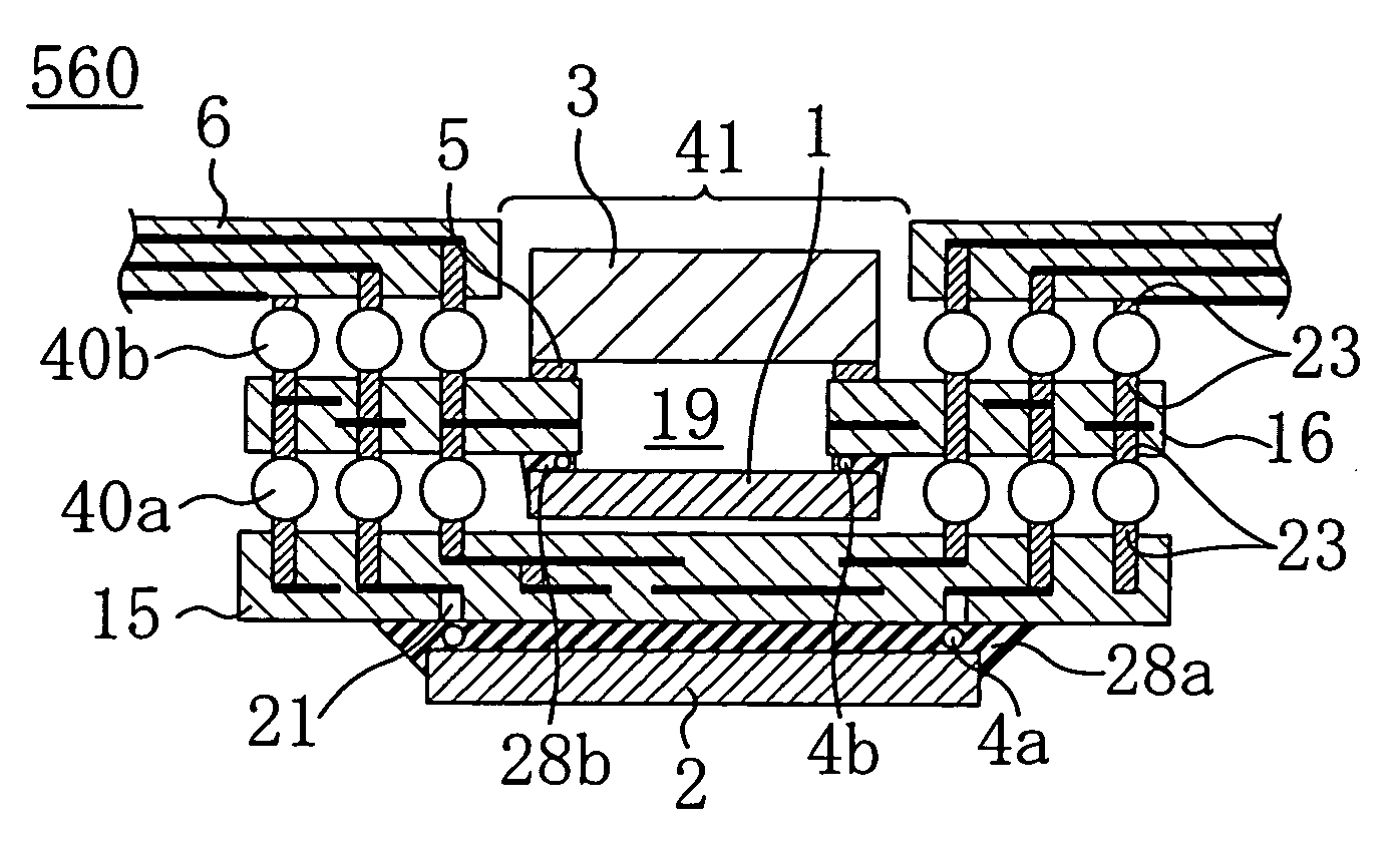
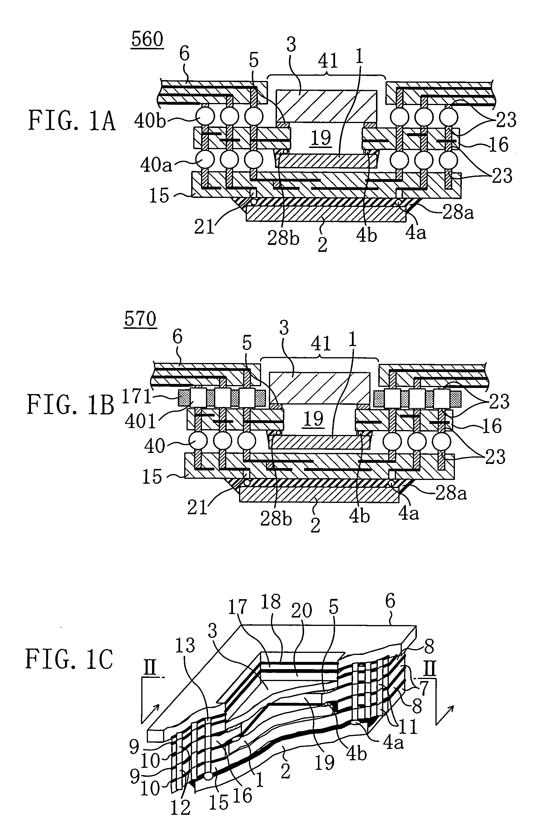
[0050] An imaging module 560 according to a first embodiment of the present invention will be described with reference to FIG. 1A.

[0051]FIG. 1A is a cross-sectional view (cross-sectional end view) illustrating an overall configuration of the imaging module 560 of this embodiment. As illustrated in FIG. 1A, the imaging module 560 of this embodiment includes: a first resin board 15; a semiconductor control chip 2 partly sealed with a sealing resin 28a at the lower surface of the first resin board 15; a second resin board 16 having an imaging opening 19 at its center region and provided over the first resin board 15 with electrically-conductive members 40a sandwiched therebetween; an imaging semiconductor chip 1 placed on the lower surface of the second resin board 16; a printed circuit board 6 having a light-receiving opening 41 and placed over the second resin board 16 with the electrically-conductive members 40b sandwiched therebetween; and an optical member 3 placed on the upper s...

embodiment 2

[0062] An imaging module 570 according to a second embodiment of the present invention will be described with reference to FIG. 1B. In this embodiment, aspects different from the first embodiment will be mainly described.

[0063]FIG. 1B is a cross-sectional view illustrating an overall configuration of the imaging module 570 of this embodiment. As illustrated in FIG. 1B, the imaging module 570 of this embodiment includes: a first resin board 15; a semiconductor control chip 2 partly sealed with a sealing resin 28a at the lower surface of the first resin board 15; a second resin board 16 having an imaging opening 19 at its center region and placed over 10 the first resin board 15 with first electrically-conductive members 40 sandwiched therebetween; an imaging semiconductor chip 1 placed on the lower surface of the second resin board 16; a printed circuit board 6 having a light-receiving opening 41 and placed above the second resin board 16; a parallel-plane member 171 sandwiched betw...

embodiment 3

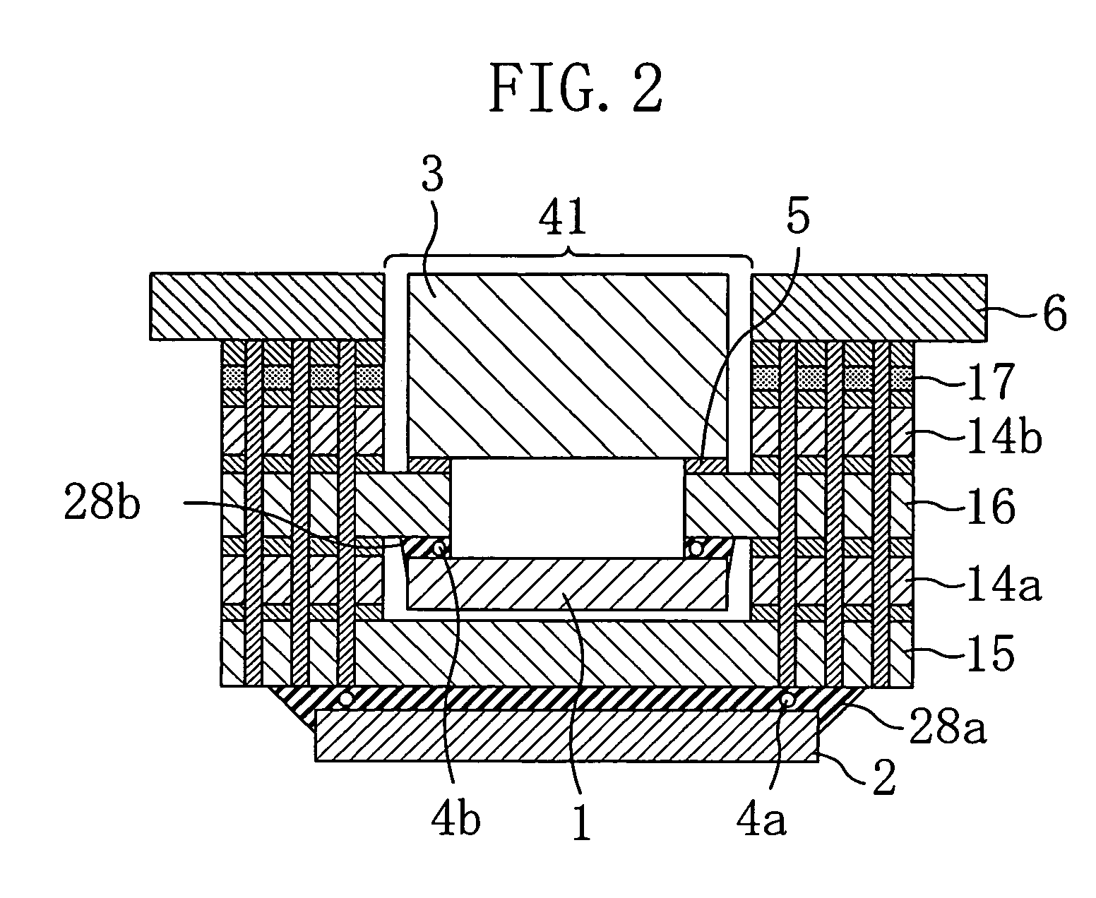
[0069]FIG. 1C is a perspective cross-sectional view schematically illustrating an overall configuration of an imaging module 500 according to a third embodiment of the present invention. FIG. 2 is a cross-sectional view of the imaging module 500 taken along the line II-II in FIG. 1C. FIGS. 3A through 3C, FIGS. 4A through 4C, FIGS. 5A and 5B, FIGS. 6A and 6B and FIGS. 7A and 7B are views illustrating components of the imaging module 500 of this embodiment. Hereinafter, the imaging module of this embodiment will be described with reference to the drawings.

—Configuration of Imaging Module—

[0070] As illustrated in FIG. 1C and FIG. 2, the imaging module 500 of this embodiment includes: a first resin board 15; a semiconductor control chip 2 partly sealed with a sealing resin 28a at the lower surface of the first resin board 15; a first sheet member 14a having an opening at its center region and adhering to the upper surface of the first resin board 15; a second resin board 16 having an i...


PUM


Abstract

An imaging module is formed by stacking: a first resin board; a second resin board having a first opening; a first electrically-conductive member electrically connecting the first resin board and the second resin board to each other; a printed circuit board having a second opening; a second electrically-conductive member electrically connecting the second resin board and the printed circuit board to each other; an imaging semiconductor chip mounted on the lower surface of the second resin board to cover the first opening and provided with an imaging sensor, an optical member placed on the upper surface of the second resin board to cover the first opening; a first semiconductor control chip provided with a control device for controlling operation of the imaging sensor and mounted on the lower surface of the first resin board.

Description

BACKGROUND OF THE INVENTION [0001] (1) Field of the Invention [0002] The present invention relates to a multilevel imaging module formed by disposing an imaging semiconductor -chip and a semiconductor control chip in three dimensions, and a method for fabricating the module. [0003] (2) Description of Related Art [0004] In recent years, there are a high demand for size reduction and functional improvement of electronic devices such as cellular phones and digital cameras. To meet this demand, multilevel semiconductor packages formed by stacking electronic components, particularly image sensor chips, and integrated circuit chips for signal processing have been proposed. [0005] For example, an imaging module having a stack package structure for electrically connecting an image sensor to a wiring board is known. This imaging module includes, for example, a board, an envelope, an integrated circuit chip, a spacer, an image sensor chip and a transparent layer. In this imaging module, a sig...

Claims


Application Information

Patent Timeline
IPC IPC(8): H01L23/02H01L27/14H04N5/335
CPCH01L27/14618H01L27/14625H01L27/14634H01L27/1469H05K1/182H01L2224/16225H01L2924/00014H01L2924/00011H04N23/57H01L2224/0401
Inventor SATOU, MOTOAKIKAWABATA, TAKESHISHINAGAWA, MASATOSHIFUKUDA, TOSHIYUKI
Owner COLLABO INNOVATIONS INC
Why Eureka
Try Eureka