Wavelength tunable semiconductor laser apparatus

a semiconductor laser and wavelength technology, applied in semiconductor lasers, electrical devices, laser details, etc., can solve the problems of difficult to achieve laser oscillation, difficult to ensure the long-term reliability of lasers in terms of wavelength, complicated control system, etc., and achieve the effect of increasing the distance lgr

Inactive Publication Date: 2006-09-14
HITACHI LTD
View PDF12 Cites 8 Cited by
  • Summary
  • Abstract
  • Description
  • Claims
  • Application Information

AI Technical Summary

Benefits of technology

[0032] The present invention has been described with reference to the case where a wide combined continuous wavelength tunable range is to be achieved. However, lasers for communications only need to generate a wavelength grid having a fixed pitch ΔλGRID, allowing the requirement expressed by the inequality (7) to be relaxed. That is, in this case, there may be wavelength ranges that are not covered by either of the two channels. Such an arrangement will be described with reference to FIG. 8. In the figure, the vertical axis represents the wavelength, and the horizontal broken lines together represent a wavelength grid having a predetermined pitch. This wavelength grid corresponds to one of the wavelength grids specified by International Telecommunication Union-Telecommunication Sector (for example, the 100 GHz pitch grid, or the approximately 0.8 nm pitch grid). Each double-arrowed vertical line indicates an oscillation wavelength range of the laser ch1 or ch2. The lasers ch1 and ch2 together cover an entire wavelength grid. Referring to the figure, in example (A), the laser ch1 covers the odd grid elements and the laser ch2 covers the even grid elements; in example (B), the laser ch1 covers the first two grid elements, the third two grid elements, and so on, and the laser ch2 covers the second two grid elements, the fourth two grid elements, and so on; in example (C), they cover three grid elements at a time in the same manner; and in example (D), they cover four grid elements at a time in the same manner. Although in every example there are wavelength ranges that are not covered by either of the two channels (that is, the above inequality (7) is not satisfied), these lasers ch1 and ch2 can together generate all the wavelengths of the entire wavelength grid and therefore these arrangements can be applied to laser devices for communications. This allows the distance Lgrt to be increased, providing an advantage over conventional arrangements in terms of laser oscillation. FIG. 9 shows exemplary wavelength characteristics of the laser channels ch1 and ch2. The wavelength grid pitch ΔλGRID is 0.8 nm and the laser channels ch1 and ch2 alternately cover two wavelength grid elements at a time. Other conditions are such that: Lgrt1=105 μm; Lgrt2=105.119 μm; Λ1=Λ2=0.238 μm; and κ=90 cm−1. In this example, the generated wavelength grid includes the wavelengths of 16 grid elements (from 1540.6 nm to 1552.6 nm).

Problems solved by technology

In order for these DBR lasers to oscillate at a desired wavelength, it is necessary to control currents to adjust not only the wavelength but also the phase of the light, resulting in a complicated control system.
Furthermore, it has been difficult to ensure the long-term reliability of the lasers in terms of wavelength.
Another problem is that increasing the continuous wavelength tunable range requires the length Lgain of the gain region 139 to be reduced, making it difficult to achieve laser oscillation. FIG. 4 shows calculated values indicating the dependence of the continuous wavelength tunable range Δλcon on the distance Lgrt.
This requirement is very difficult to meet if laser oscillation is to be produced.
Therefore, practically, such a structure is not suitable for mass production.

Method used


Image

  • Wavelength tunable semiconductor laser apparatus
  • Wavelength tunable semiconductor laser apparatus
  • Wavelength tunable semiconductor laser apparatus

Examples


first embodiment

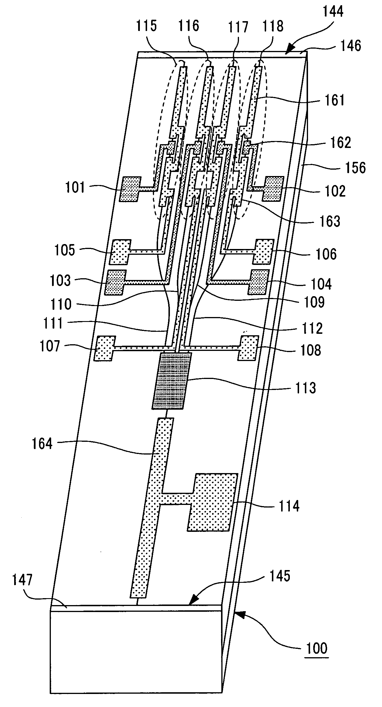
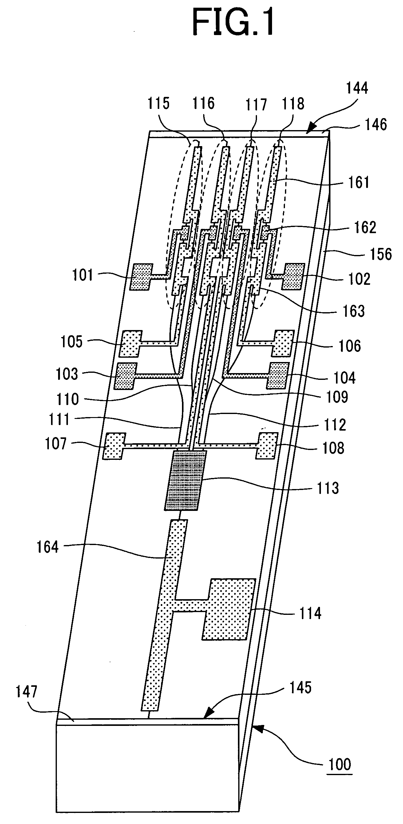
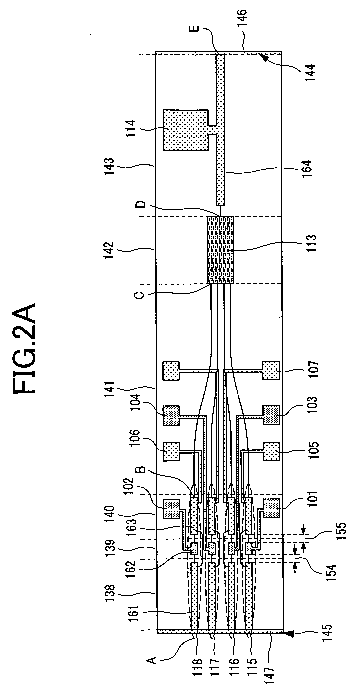
[0059] There will now be described an exemplary wavelength tunable semiconductor device whose oscillation wavelength can be varied by injecting a current into the refractive index control layer and selecting one of the DBR laser channels. This semiconductor laser device oscillates at wavelengths within the 1550 nm band. FIGS. 10, 11A, and 11B show the exemplary semiconductor laser device. FIG. 10 is a perspective view; FIG. 11A is a top view; and FIG. 11B is a cross-sectional view taken along line F-G-H-I-J of FIG. 11A. Specifically, like FIG. 2B above (showing a cross section taken along line A-B-C-D-E), FIG. 11B shows a cross section taken along an optical path that passes through the semiconductor laser portion (shown in the upper left of the figure), the gate region, an optical waveguide, the optical combiner for combining the light waves from a plurality of optical waveguides, and the semiconductor optical amplifier. The channel DBR laser array, the MMI combiner, and the SOA ar...

second embodiment

[0069] With reference to FIGS. 13A and 13B, there will now be described another exemplary wavelength tunable semiconductor device for the 1550 nm band whose oscillation wavelength can be varied by injecting a current into the refractive index control layer and selecting one of the DBR laser channels. FIG. 13A is a top view of the device and FIG. 13B is a cross-sectional view taken along line F-G-H-I-J of FIG. 13A.

[0070] The second embodiment is different from the first embodiment in that the laser device of the second embodiment does not include the rear DBR region 138 but instead includes a high reflective film 201 formed on a semiconductor end face. All other components are basically similar to those described with reference to the first embodiment. It should be noted that eliminating the rear DBR region 138 allows the DBR current to be reduced to approximately half. The symbol Lgrt1 denotes the distance between the high reflective film 201 of the DBR laser channel ch1 (or 115) a...

third embodiment

[0073]FIG. 15 shows the wavelength characteristics of a laser device adapted to generate a wavelength grid having a fixed pitch ΔλGRID. The dimensions of the device and its manufacturing method were the same as those of the first embodiment. The basic structure of the device is similar to that shown in FIGS. 10, 11A, and 11B.

[0074] The following description will be directed primarily to the laser channels ch1 and ch2. In order to allow the channels ch1 and ch2 to achieve a grid pitch ΔλGRID of 0.8 nm and alternately cover two wavelength grid elements at a time, these channels were formed such that: Lgrt1=105 μm; Lgrt2=105.119 μm; Λ1=Λ2=0.238 μm; and κ1=κ2=κ3=κ4 =90 cm−1. As a result, even though there are wavelength ranges that were not covered by either of the two channels, these channels alternately covered two wavelength grid elements at a time, and the resultant wavelength grid included 16 grid elements (from 1540.6 nm to 1552.6 nm).

[0075] There will now be described how to de...


PUM


Abstract

The present invention relates to wavelength tunable DBR semiconductor laser devices in which light waves generated from a plurality of laser portions (or laser channels) are combined. This type of semiconductor laser device requires that the laser channels together cover an entire desired wavelength range, allowing the oscillation wavelength to be continuously varied over this range. However, to accomplish this, it is necessary to employ highly accurate crystal growth and process techniques. Furthermore, the length of the gain region must be reduced to increase the range over which the oscillation wavelength can be continuously varied, making it difficult to achieve laser oscillation.
Two laser channels operate in combination, and a combiner combines the light waves emitted from these laser portions (or laser channels) so as to cover one entire wavelength range. Specifically, an inter-grating element distance Lgrt1 of the first laser portion is set larger or smaller than an inter-grating element distance Lgrt2 of the second laser portion by one half of the grating pitch. This allows these laser portions to exhibit different mode-hopping DBR current values appropriately adjusted against each other and thereby together cover a desired wavelength range.

Description

CLAIM OF PRIORITY [0001] The present application claims priority from Japanese application JP 2005-070376 filed on Mar. 14, 2005, the content of which is hereby incorporated by reference into this application. FIELD OF THE INVENTION [0002] The present invention relates to a semiconductor laser device in which a plurality of generated laser beams are combined to output laser light, and more particularly to an arrayed distributed Bragg reflector (DBR) laser device capable of operating as a wavelength tunable semiconductor laser to provide a given wavelength of light. BACKGROUND ART [0003] DBR lasers having a special grating such as an SG (Sampled Grating) or SSG (Super Structure Grating) have been developed for use as wavelength tunable semiconductor lasers to provide any wavelength within the C-band used in wavelength division multiplexer (WDM) systems. In order for these DBR lasers to oscillate at a desired wavelength, it is necessary to control currents to adjust not only the wavel...

Claims


Application Information

Patent Timeline
Patent Type & Authority Applications(United States)
IPC IPC(8): H01S3/10
CPCH01S5/026H01S5/0265H01S5/06256H01S5/1039H01S5/125H01S5/4068
Inventor ARIMOTO, HIDEO
Owner HITACHI LTD
Why Eureka
Try Eureka