Monolithic microchip laser with intracavity beam combining and sum frequency or difference frequency mixing
a microchip laser and intracavity beam technology, applied in the field of solid-state lasers, can solve the problems of high cost, long-term reliability problems, and large volume of lasers, and achieve compact and cost-effective manner, suppressing unwanted polarization, and high-volume manufacturing
- Summary
- Abstract
- Description
- Claims
- Application Information
AI Technical Summary
Benefits of technology
Problems solved by technology
Method used
Image
Examples
example 1
Monolithic Microchip Laser for Generating 491.7 nm Light
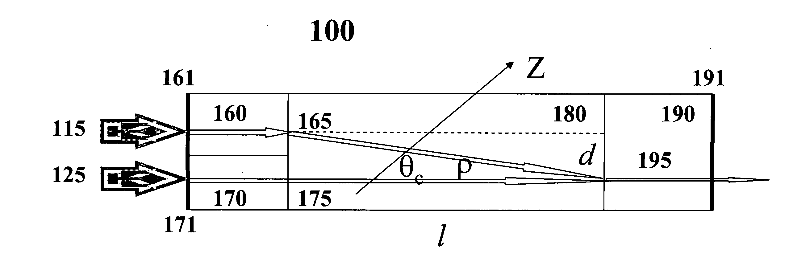
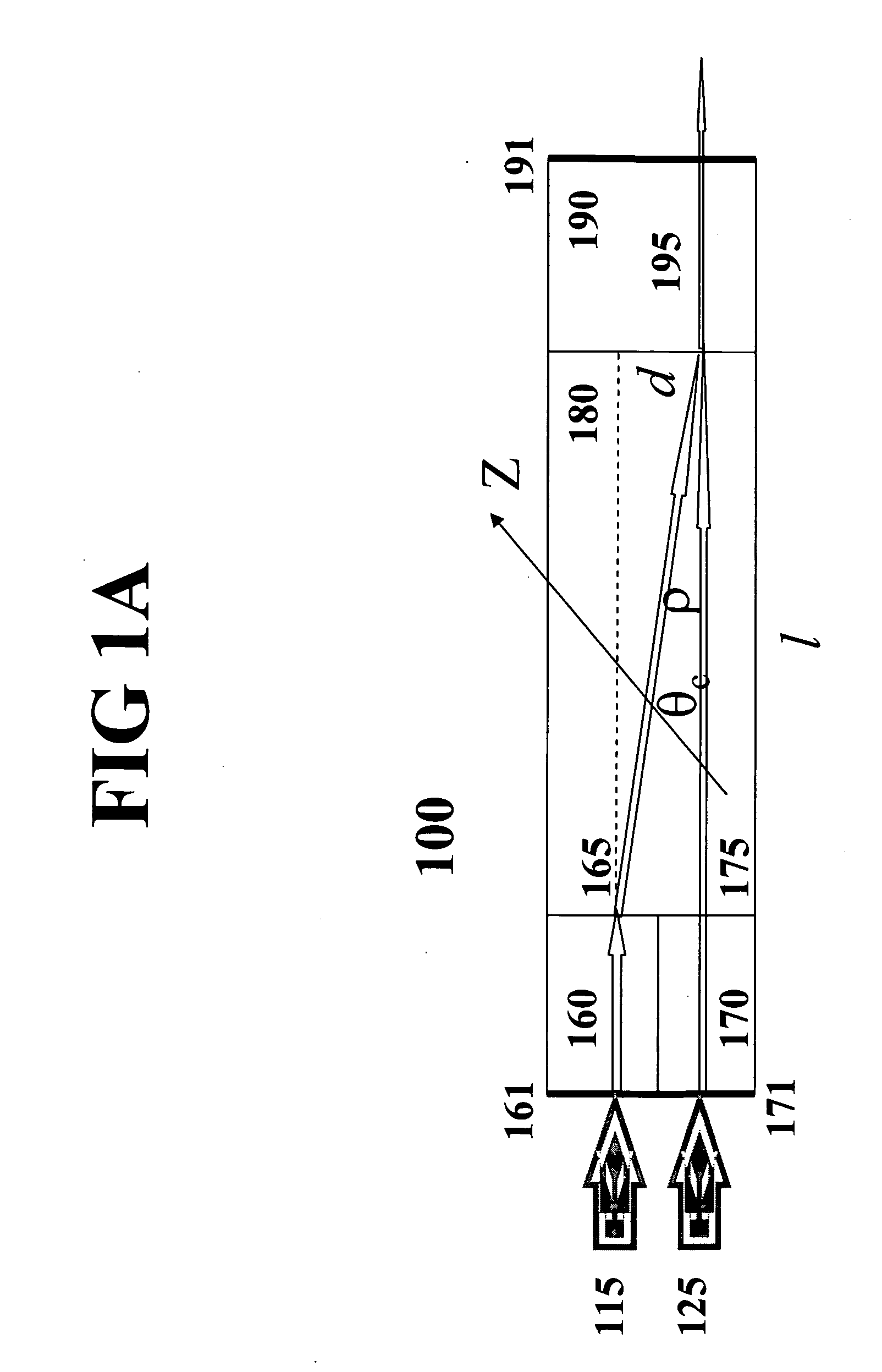
[0076] Returning to FIG. 1A. In this specific example, the monolithic microchip laser 100 consists of two independent pumping sources 115 and 125, two Nd:YVO4 laser gain media 160 and 170, a birefringent crystal such as un-doped YVO4 or TiO2 180, and a nonlinear crystal KTP 190. These crystals are optically bonded and in physical contact for elimination of the boundary optical loss in generation of intracavity SFM or DFM.
[0077] In a preferred embodiment, the pumping lights 115 and 125 are output from a build-in dual-emitter diode laser that emits two individual laser beams, but can also from two separate emitter diode lasers, depending on specific applications. Each emitter can have a 1 μm×50 μm aperture and emit upto 500 mW power output at 808 nm or have 1 μm×200 μm aperture and emit upto 2 W power output at 808 nm or other aperture size to emit an appropriate power. These two emitters are separated each other with a prefera...
example 2
Monolithic Microchip Laser for Generating 593.5 nm Light
[0082] Continuing in reference to FIG. 1A. With modification of some parameters, the same configuration can be applied to other wavelength conversion devices, e.g., 593.5 nm lasers. These parameters include proper selection of mirror coatings and KTP phase matching angle.
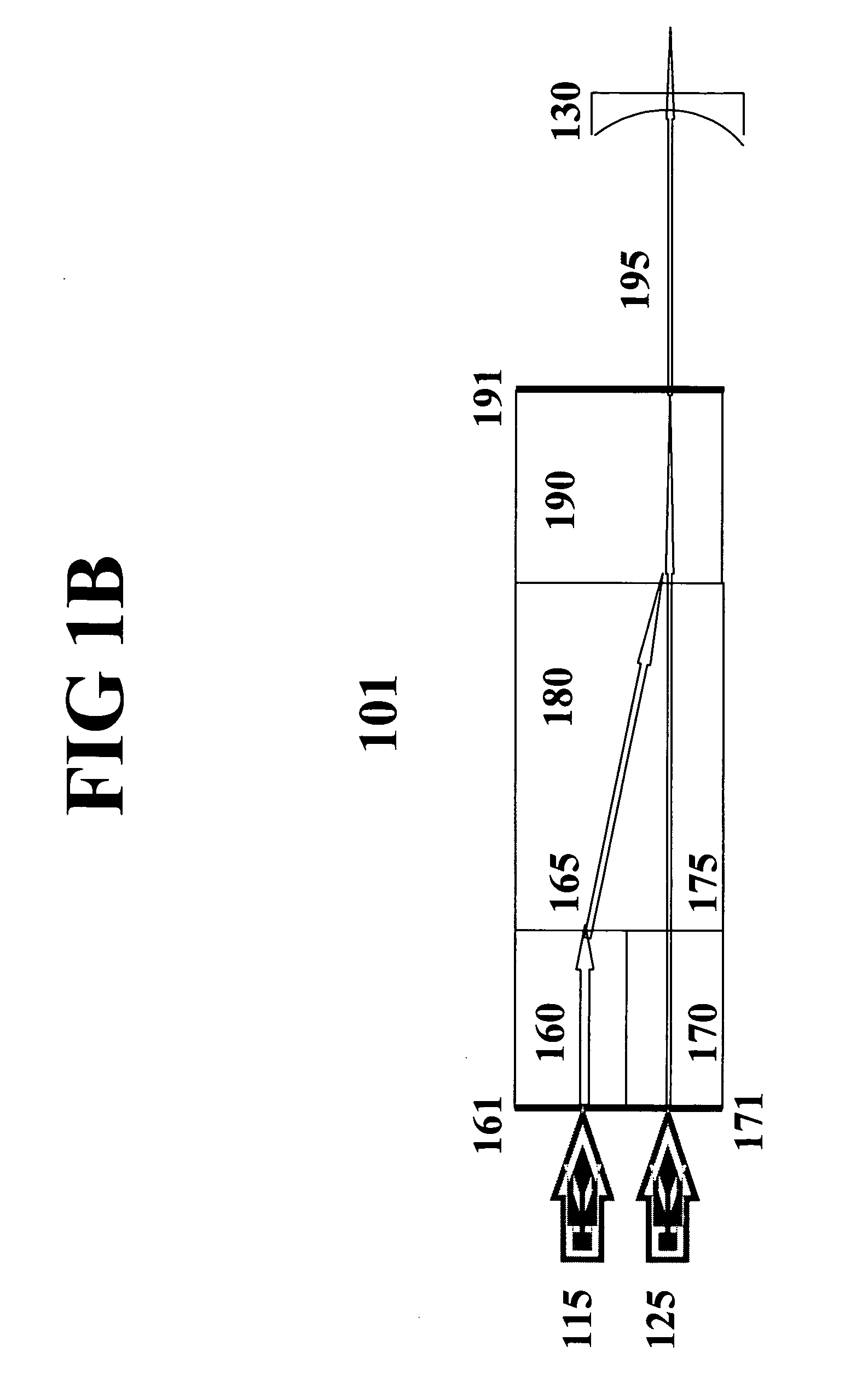
[0083] In order to generate laser output at 593.5 nm, the coating 161 should be highly reflective at 1064 nm and highly transmissive (T>95%) at 808 nm. Similarly, the mirror 171 is coated HR at 1342 nm and HT at 808 nm. The coating 171 is also HT at 1064 nm to prevent this high-gain transition from lasing. The coating 191 on the exterior surface of microchip 100 is HT at 593.5 nm, and HR at both 1342 and 1064 nm. In some applications, configurations illustrated in FIG. 1B or 1C or 1E or 1F can be used.
[0084]FIG. 3B shows a flowchart of the wavelength conversion. Advantageously, an algorithm for automatic power control enables individual adjustment of pumping...
PUM
 Abstract
Description
Claims
Application Information


