

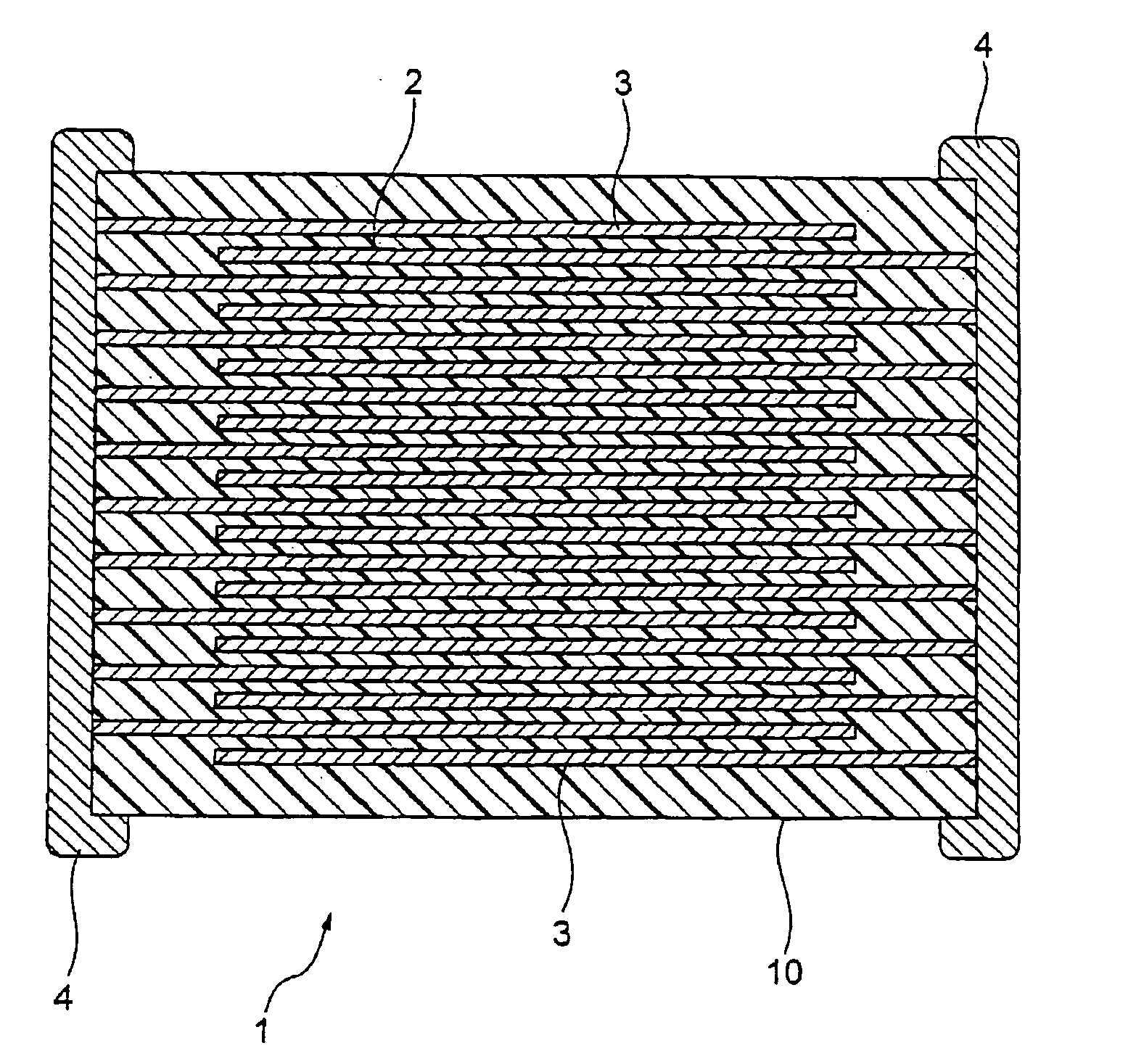
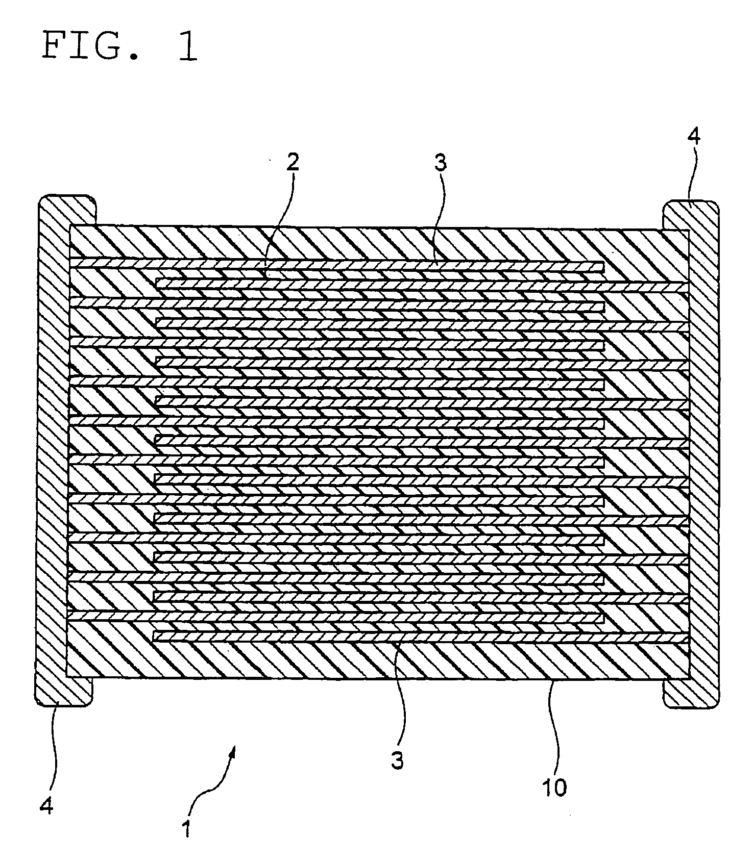
Method of production of multilayer ceramic electronic device
a technology of electronic devices and ceramics, applied in the manufacture of capacitors, fixed capacitors, thin/thick film capacitors, etc., can solve the problems of inability to suitably control the treatment temperature and oxygen partial pressure in the annealing atmosphere, the dielectric ratio of recent capacitors is being increasingly reduced, and the capacitors are difficult to produce superior in various types of characteristics, etc., to reduce the end oxidation of internal electrode layers and reduce the effect of capacity fluctuation
- Summary
- Abstract
- Description
- Claims
- Application Information
AI Technical Summary
Benefits of technology
Problems solved by technology
Method used
Image

Examples
example 1
[0111] Preparation of Dielectric Material
[0112] First, the barium titanate material, glass ingredient material, and additive ingredient material were prepared.
[0113] As the barium titanate material, BaTiO3 with an average crystal grain size of 0.35 μm was used.
[0114] As the glass ingredient material, BaO, CaO, and SiO2 were used.
[0115] As the additive ingredient material, MgO, MnO, Y2O3, and V2O5 of an average particle size of 0.01 to 0.1 μm were used.
[0116] Next, to 100 mol of the barium titanate material, the glass ingredient material constituted by BCG and the additive ingredient material constituted by MgO, MnO, Y2O3, and V2O5 were added. These were wet mixed using water as a solvent by a ball mill for 16 hours (water crushing). Then, hot air was blown for drying at 130° C. to obtain a dielectric material.
[0117] The dielectric material contained, with respect to 100 mol of the barium titanate material, BaO and CaO in amounts of 4 mol each, SiO2 in an amount of 4 mol, MgO i...
example 2
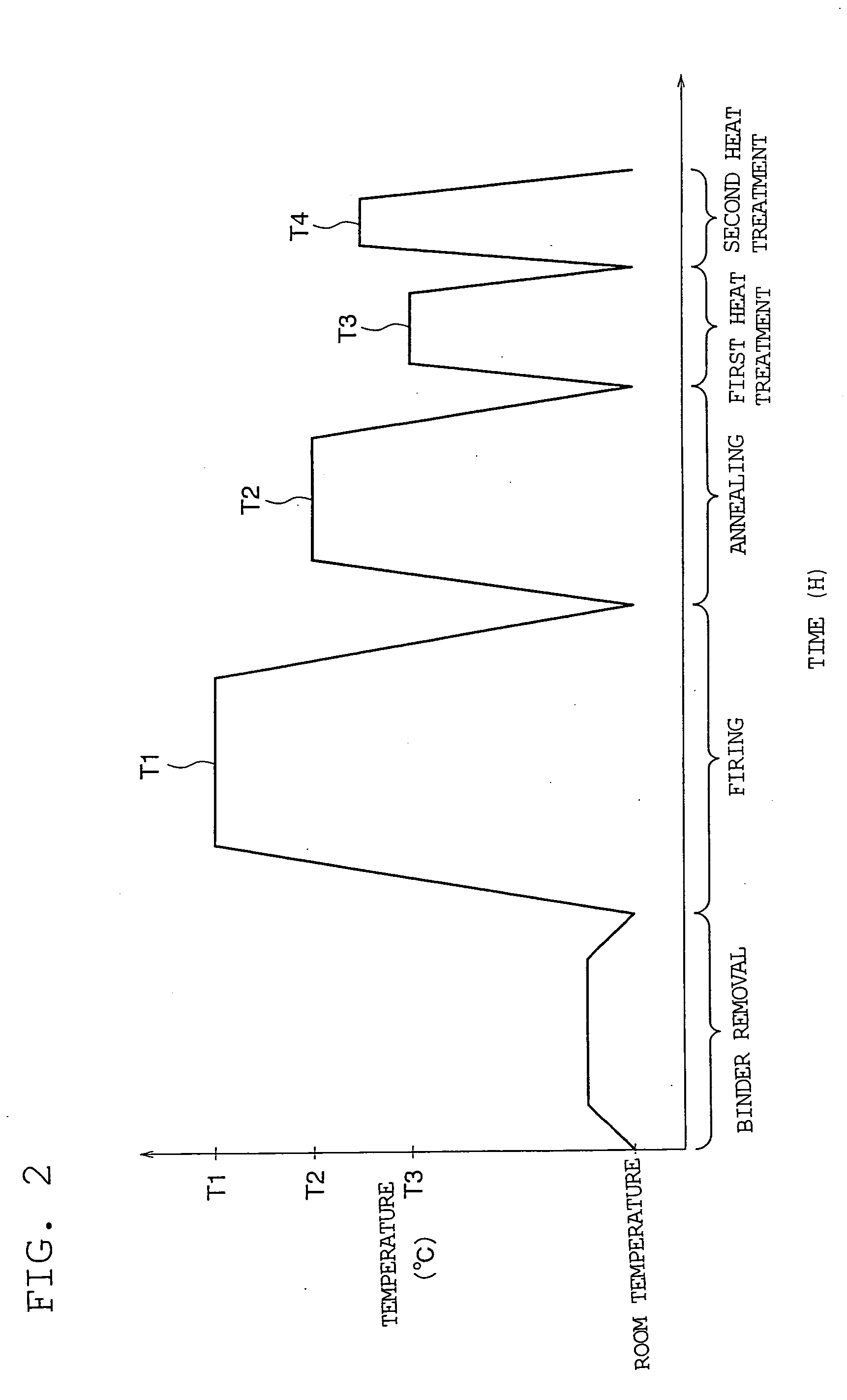
[0183] Except for changing the T3 holding time of the first heat treatment and the T4 holding time of the second heat treatment from zero (no keep) to 24 hours, a capacitor sample was prepared and evaluated under the same conditions as Sample 5 shown in Table 1 of Example 1. As a result, similar results are obtained.
example 3
[0184] Except for changing the rate of temperature rise of the first heat treatment and the rate of temperature rise of the second heat treatment 300° C. / hour and 1000° C. / hour, a capacitor-sample was prepared and evaluated under the same conditions as Sample 5 shown in Table 1 of Example 1. As a result, similar results are obtained as with the case of a rate of temperature rise of 500° C. / hour.
PUM
| Property | Measurement | Unit |
|---|---|---|
| thickness | aaaaa | aaaaa |
| holding temperature | aaaaa | aaaaa |
| holding temperature | aaaaa | aaaaa |
Abstract
Description
Claims
Application Information