Semiconductor device

a technology of semiconductor devices and semiconductors, applied in semiconductor devices, capacitors, electrical devices, etc., can solve the problems of not increasing the thickness of the whole structure, etc., to prevent the thickness of the whole device from being increased, effectively inhibited, and not encouraging surface unevenness

Inactive Publication Date: 2006-10-05
LAPIS SEMICON CO LTD
View PDF5 Cites 20 Cited by
  • Summary
  • Abstract
  • Description
  • Claims
  • Application Information

AI Technical Summary

Benefits of technology

[0010] It is therefore an object of the present invention to resolve the above-described problem, and to provide a semiconductor device which inhibits chemical reactions between the Al of a wiring film and the Pt of an electrode, and prevents the thickness of the whole device from being increased. A semiconductor device in accordance with the present invention comprises a semiconductor substrate, a first electrode that is formed over said semiconductor substrate, a capacitive insulating film that is formed on said first electrode and which comprises a metal oxide ferroelectric, a second electrode that is formed on said capacitive insulating film, an insulating film that has a first opening exposing a portion of an upper side of said second electrode and is formed so as to cover said first electrode, said capacitive insulating film, and said second electrode, a first barrier film with an amorphous structure which is formed inside said first opening and on said insulating film, and a wiring film that is formed over said first barrier film.
[0011] The semiconductor device in accordance with the present invention includes an amorphous structure, that is, a first barrier film having a structure in which a crystal grain boundary does not exist, between a second electrode (i.e., an upper electrode of a capacitor) and a wiring film. Because of this, the diffusion of Al, the main material of a wiring film, can be prevented, and chemical reactions between Al and Pt (the material of an electrode) can be effectively inhibited. Also, in the semiconductor device of the present invention, a first barrier is formed as a portion of a wiring structure. Therefore, surface unevenness is not encouraged, and the thickness of the whole structure is not increased, by forming a first barrier film.

Problems solved by technology

Therefore, surface unevenness is not encouraged, and the thickness of the whole structure is not increased, by forming a first barrier film.

Method used


Image

  • Semiconductor device
  • Semiconductor device
  • Semiconductor device

Examples


first embodiment

[0039] Capacitor Structure and Wiring Structure

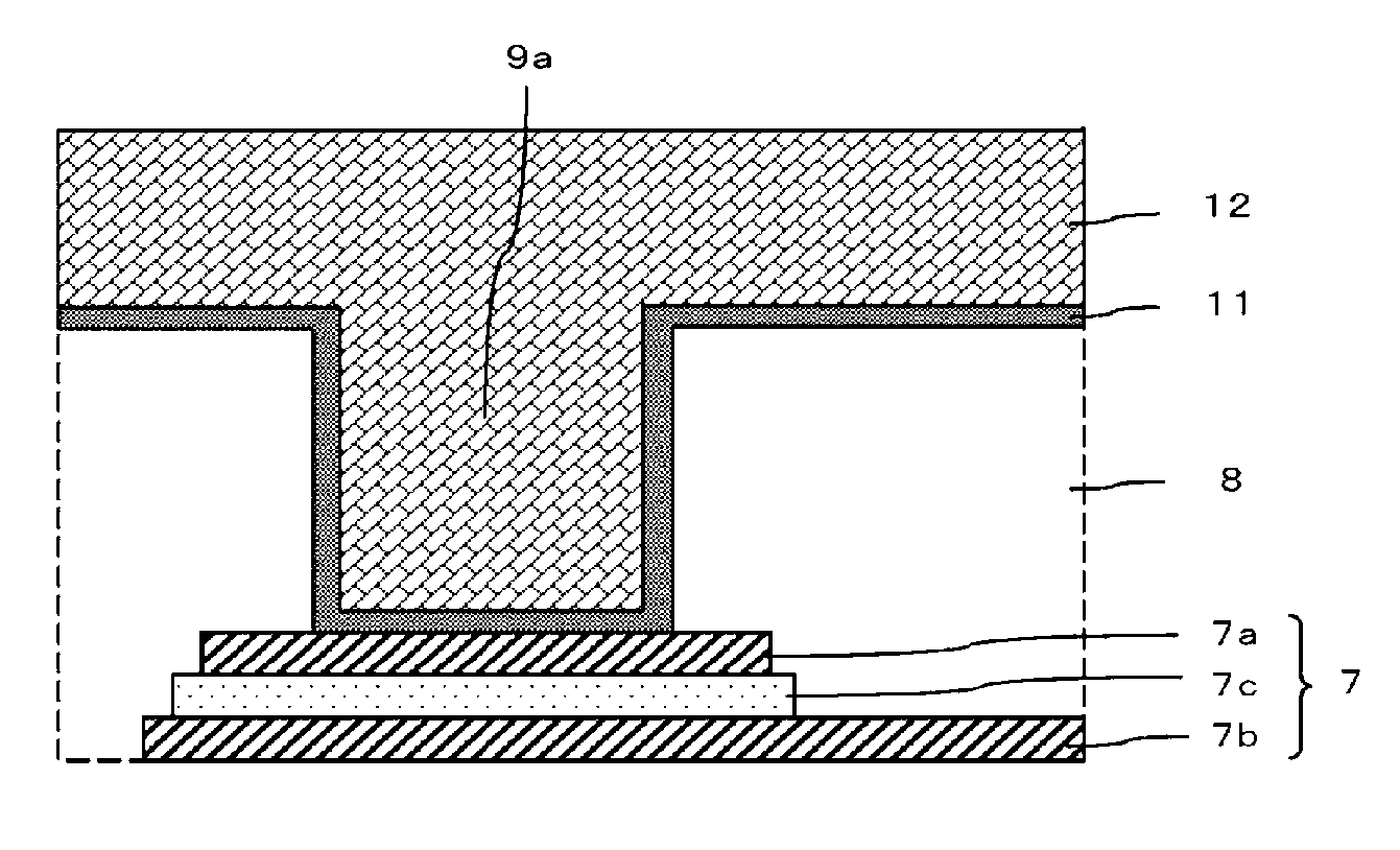
[0040]FIG. 1 is a schematic diagram showing a ferroelectric capacitor and its wiring structure in a semiconductor device in accordance with a first embodiment of the present invention.

[0041] An upper electrode 7a and a lower electrode 7b are capacitor electrodes composed of material with excellent oxidation resistance. For example, the material consists primarily of Pt. A capacitive insulating film 7c is a metal-oxide ferroelectric. For example, it is comprised of strontium bismuth tantalum oxide (SBT or SrBi2Ta2O9). A ferroelectric capacitor 7 is comprised of a laminated structure of the lower electrode 7b, the capacitive insulating film 7c formed on the lower electrode 7b, and the upper electrode 7a formed on the capacitive insulating film 7c.

[0042] An insulating film 8 is an interlayer insulating film that covers the ferroelectric capacitor 7. For example, it is comprised of a silicon dioxide film. A contact 9a is a connector for ...

second embodiment

[0065] Capacitor Structure and Wiring Structure

[0066]FIG. 9 is a schematic diagram showing a ferroelectric capacitor and its wiring structure in a semiconductor device in accordance with a second embodiment of the present invention. The ferroelectric capacitor and its wring structure in FIG. 9 include some elements that are also shown in FIG. 1. Therefore, each of these elements in FIG. 9 has the same number and / or symbol that are assigned to the corresponding elements in FIG. 1, and the description thereof will be partially omitted here.

[0067] A contact 9a is a connector for electrically connecting the ferroelectric capacitor 7 and external elements. The contact 9a is formed so as to be in contact with the upper electrode 7a through a barrier film 14 and a reaction film 15 as a portion of a wiring film 12 formed on an insulating film 8. The barrier film 14 is a conducting film with an amorphous structure which inhibits chemical reactions between the upper electrode 7a and the wir...

third embodiment

[0077] Capacitor Structure and Wiring Structure

[0078]FIG. 11 is a schematic diagram showing a ferroelectric capacitor and its wiring structure in a semiconductor device in accordance with a third embodiment of the present invention. The ferroelectric capacitor and its wring structure in FIG. 11 include some elements that are also shown in FIG. 1. Therefore, each of these elements in FIG. 11 has the same number and / or symbol that are assigned to the corresponding elements in FIG. 1, and the description thereof will be partially omitted here.

[0079] A contact 9a is a connector for electrically connecting the ferroelectric capacitor 7 and external elements. The contact 9a is formed so as to be in contact with the upper electrode 7a through barrier films 16, 17, and 18 as a portion of a wiring film 12 formed on an insulating film 8. The barrier films 16, 17, and 17 are conducting films which inhibit chemical reactions between the upper electrode 7a and the wiring film 12. They are requ...


PUM


Abstract

A semiconductor device includes a semiconductor substrate, a first electrode that is formed over said semiconductor substrate, a capacitive insulating film that is formed on the first electrode and is made of a metal oxide ferroelectric, a second electrode that is formed on the capacitive insulating film, an insulating film that has a first opening exposing a portion of an upper side of the second electrode and is formed so that it covers the first electrode, the capacitive insulating film, and the second electrode, a first barrier film having an amorphous structure which is formed inside the first opening and on the insulating film, and a wiring film that is formed over the first barrier film.

Description

BACKGROUND OF THE INVENTION [0001] 1. Field of the Invention [0002] The present invention relates to a semiconductor device with a wiring structure having good electrical properties in a connection with a capacitor that uses a metal-oxide dielectric. [0003] A ferroelectric random access memory (FeRAM) is a high-speed nonvolatile memory using the hysteresis property of a ferroelectric material. A FeRAM has excellent features, such as high-speed read / write operations that are as fast as a dynamic random access memory (DRAM) and lower power consumption, for instance. [0004] When a capacitor is formed with a ferroelectric material of a metal oxide, an annealing treatment in an oxygen atmosphere at a high temperature (600-800 degrees Celsius) is required to recover the properties of the ferroelectric material after sintering or etching. Because of this, precious metal such as platinum (Pt) or iridium (Ir) having excellent oxidization resistance properties is used for the upper and lower ...

Claims


Application Information

Patent Timeline
Patent Type & Authority Applications(United States)
IPC IPC(8): H01L29/94
CPCH01L21/2855H01L28/75H01L21/31055H01L21/31116H01L21/31122H01L21/32136H01L21/76843H01L21/76846H01L21/76856H01L21/76858H01L21/76864H01L21/7687H01L21/76877H01L27/11502H01L27/11507H01L28/65H01L21/28556H10B53/30H10B53/00
Inventor ABE, KAZUHIDE
Owner LAPIS SEMICON CO LTD
Why Eureka
Try Eureka