

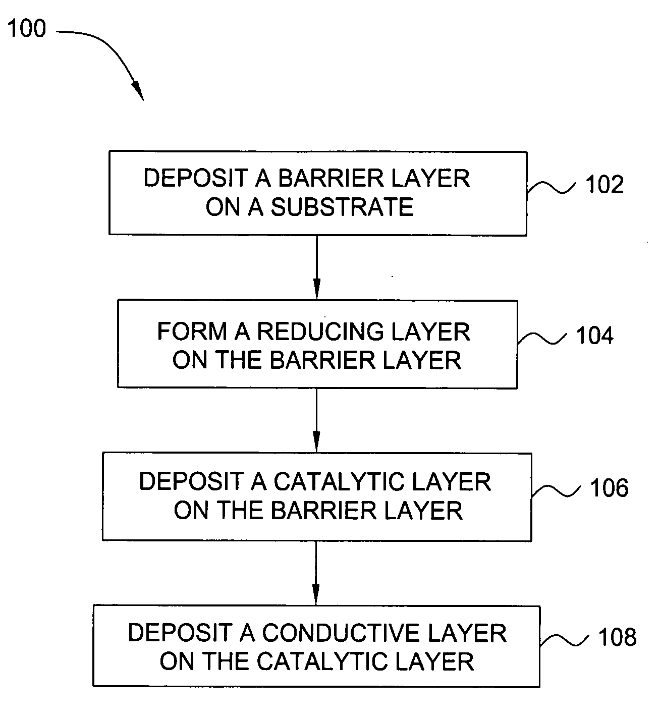
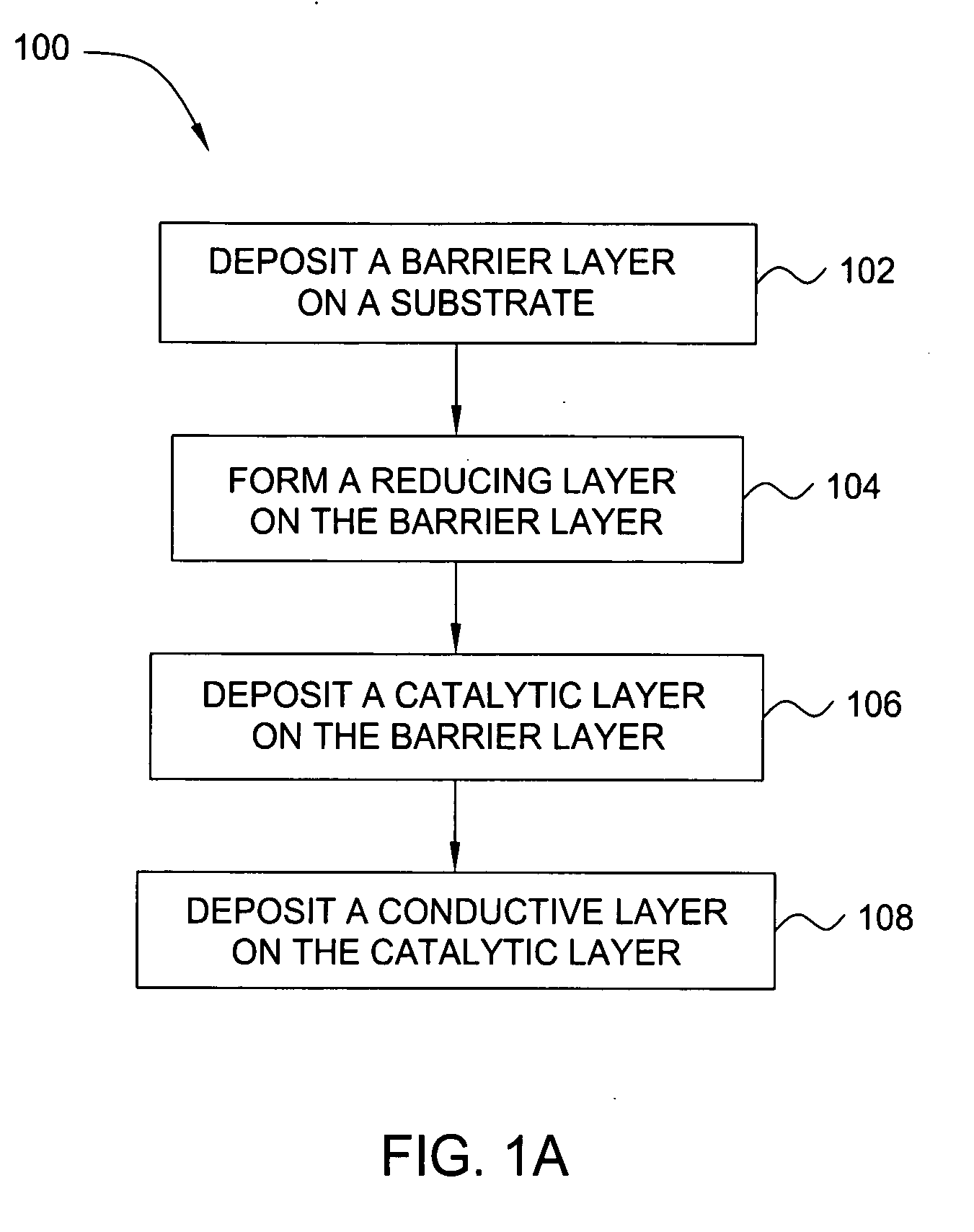
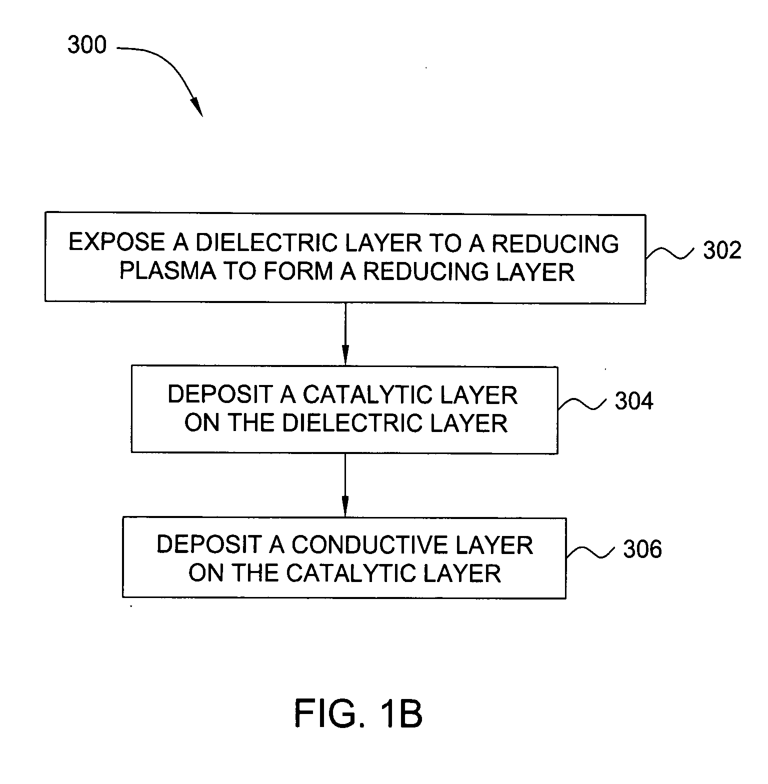
Deposition of an intermediate catalytic layer on a barrier layer for copper metallization
a catalytic layer and barrier layer technology, applied in liquid/solution decomposition chemical coatings, coatings, solid-state devices, etc., can solve the problems of copper diffusing into neighboring layers, dielectric layers becoming conductive, electronic devices failing,
- Summary
- Abstract
- Description
- Claims
- Application Information
AI Technical Summary
Problems solved by technology
Method used
Image

Examples
process example
Chamber Process Example
[0108] In one embodiment of process 100, the step 104 (e.g., forming a reducing layer) is performed in the fluid processing cell 500 just prior to completing the processing step 106, (e.g., forming a catalytic layer) in the fluid processing cell 500. In one example, the substrate is transferred into the fluid processing cell 500 and placed on the substrate receiving surface 514 by a robot (not shown) and the lift pins 518 during process 100. Next the processing shield 150 is then moved into position where it contacts the substrate receiving surface 514, or the substrate surface, to form the processing region 155. The pressure in the evacuation region 153, and processing region 155, is then lowered by use of the pump (not shown) in waste source system 151. A processing fluid is then delivered to the processing region 155 from a process gas source 161 that is connected to the injection port 144. In one example, the processing gas contains ruthenium tetroxide to ...
PUM
| Property | Measurement | Unit |
|---|---|---|
| time | aaaaa | aaaaa |
| time | aaaaa | aaaaa |
| time | aaaaa | aaaaa |
Abstract
Description
Claims
Application Information