

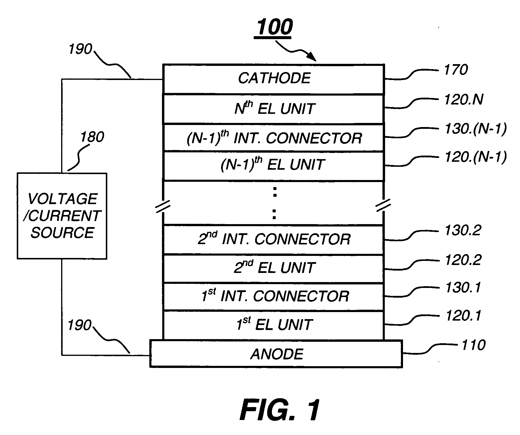
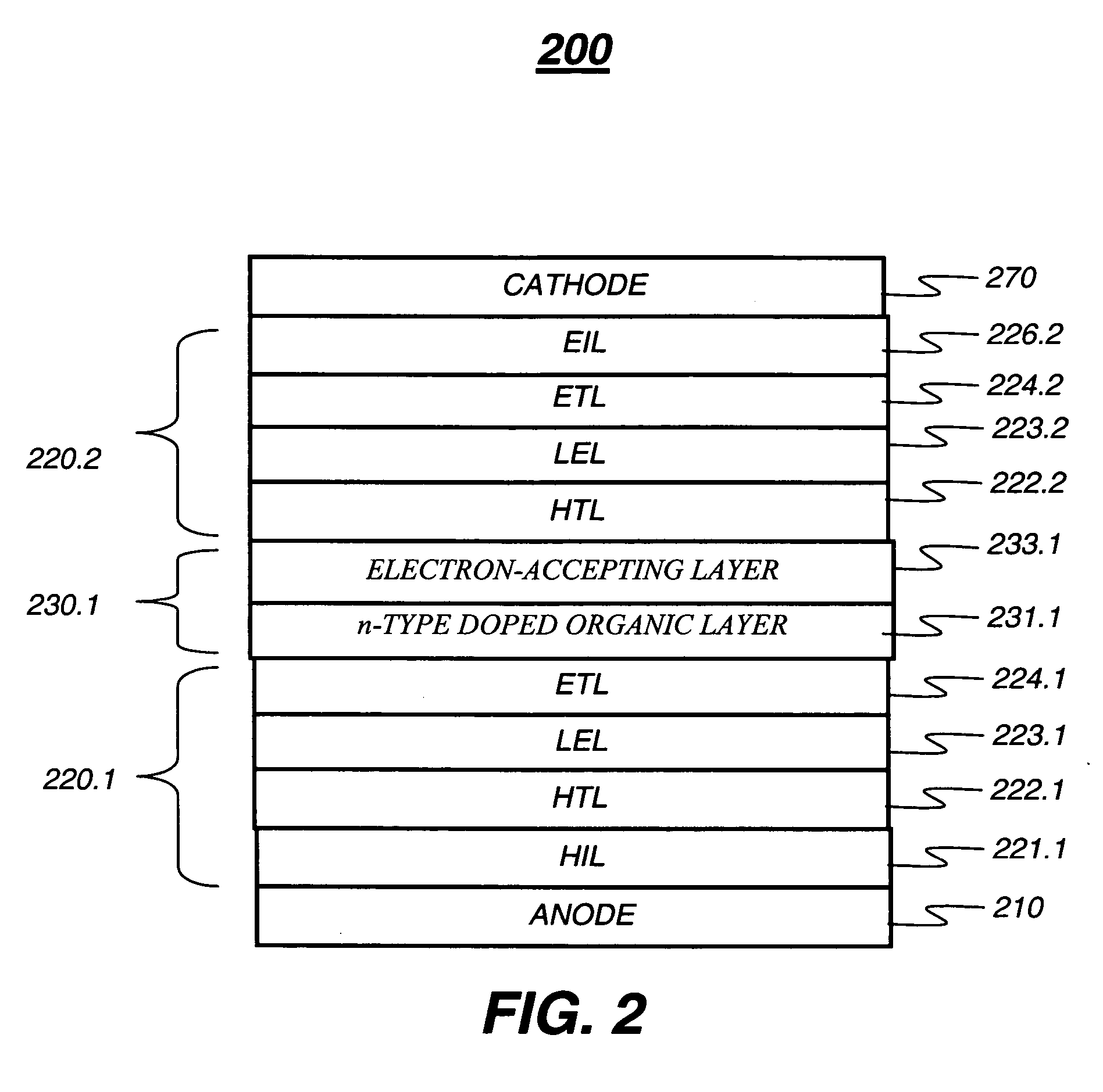
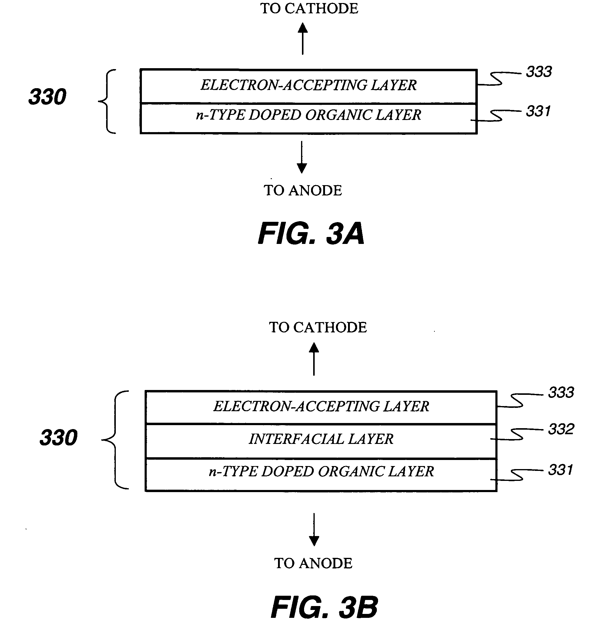
OLED device with improved performance
a technology of electroluminescent devices and electroluminescent tubes, which is applied in the direction of discharge tube luminescnet screens, other domestic articles, natural mineral layered products, etc., can solve the problems of increased drive voltage, limited voltage available, and short lifetime, and achieves low drive voltage and long lifetime. , the effect of high efficiency
- Summary
- Abstract
- Description
- Claims
- Application Information
AI Technical Summary
Benefits of technology
Problems solved by technology
Method used
Image

Examples
example 1
Comparative
[0123] The preparation of a conventional OLED is as follows:
[0124] A ˜1.1 mm thick glass substrate coated with a transparent indium-tin-oxide (ITO) conductive layer was cleaned and dried using a commercial glass scrubber tool. The thickness of ITO was about 42 nm and the sheet resistance of the ITO was about 68 Ω / square. The ITO surface was subsequently treated with oxidative plasma to condition the surface as an anode. A layer of CFx, 1 nm thick, was deposited on the clean ITO surface as the hole-injecting layer by decomposing CHF3 gas in an RF plasma treatment chamber. The substrate was then transferred into a vacuum deposition chamber for deposition of all other layers on top of the substrate. The following layers were deposited over the CFx layer in the following sequence by evaporation from heated boats under a vacuum of approximately 10−6 Torr:
[0125] a) as HTL, a 60 nm thick layer of 4,4′-Bis[N-(1-naphthyl)-N-phenylamino]biphenyl (NPB);
[0126] b) as a yellow ligh...
example 2
Comparative
[0131] An OLED was constructed with similar fabrication methods to those used in Example 1, except that the EIL was made using 25 nm 4,7-diphenyl-1,10-phenanthroline (also known as bathophen or Bphen) as the electron-transporting material which was doped with 1% by volume Li. The EL performance data are summarized in Table 1.
examples 3 and 4
[0132] Examples 3 and 4 were similar to Example 2 except that the Bphen contained 2% and 3% by volume Li, respectively. The EL performance data are summarized in Table 1.
PUM
| Property | Measurement | Unit |
|---|---|---|
| work function | aaaaa | aaaaa |
| reduction potential | aaaaa | aaaaa |
| thickness | aaaaa | aaaaa |
Abstract
Description
Claims
Application Information