
Semiconductor encapsulating epoxy resin composition and semiconductor device

Active Publication Date: 2006-10-26
SHIN ETSU CHEM IND CO LTD
View PDF6 Cites 8 Cited by
  • Summary
  • Abstract
  • Description
  • Claims
  • Application Information

AI Technical Summary

Benefits of technology

[0007] An object of the present invention is to provide an epoxy resin composition which has good flow, a low coefficient of linear expansion, a high glass transition temperature, minimal moisture absorption, crack resistance on lead-free soldering, flame retardance, and moisture-proof reliability. Another object is to provide a semiconductor device encapsulated with the epoxy resin composition in the cured state.
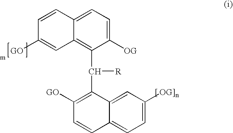
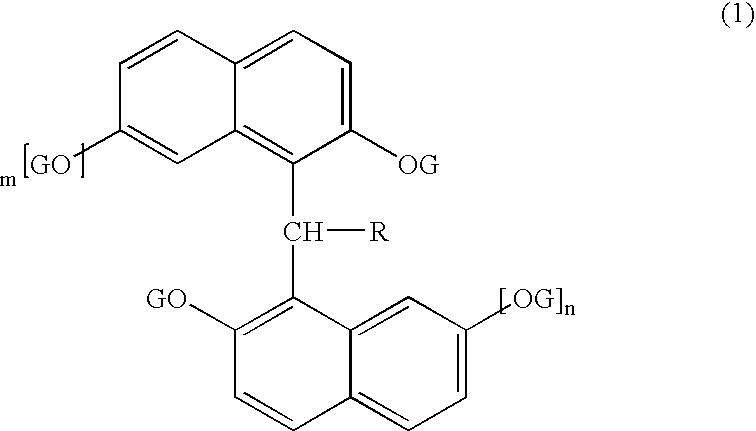
[0008] The inventor has found that by combining a specific epoxy resin of the general formula (1), shown below, with a specific phenolic resin, especially of the general formula (3), shown below, there is obtained an epoxy resin composition which is fully flowable and cures into parts having a low coefficient of linear expansion, a high glass transition temperature (Tg), and minimal moisture absorption, and that by further adding a phosphazene compound of the compositional formula (2), shown below, the composition is improved in flame retardance and moisture-proof reliability without a need for brominated epoxy resins and antimony trioxide. The composition is thus suited for semiconductor encapsulation.
[0016] The epoxy resin composition of the invention is fully flowable and cures into parts having a low coefficient of linear expansion, a high Tg, minimal moisture absorption, and crack resistance as well as flame retardance and moisture-proof reliability. It is best suited for semiconductor encapsulation. The semiconductor device encapsulated with a cured product of the epoxy resin composition is of great worth in the industry.

Problems solved by technology

For these packages which are encapsulated only on one surface, the problem of warpage after molding becomes more serious.
Thus there are left outstanding problems of delamination at the interface between the cured epoxy resin and the substrate and at the interface between the semiconductor chip and the resin paste after solder reflow.
Regrettably, a concomitant increase of viscosity can compromise the flow during molding.

Method used


Image

  • Semiconductor encapsulating epoxy resin composition and semiconductor device
  • Semiconductor encapsulating epoxy resin composition and semiconductor device
  • Semiconductor encapsulating epoxy resin composition and semiconductor device

Examples


example

[0053] Examples and Comparative Examples are given below for further illustrating the invention, but are not intended to limit the invention. All parts are by weight.

synthesis example a

[0055] In a nitrogen atmosphere, 8.6 g (214 mmol) of sodium hydride was suspended in 50 ml of tetrahydrofuran (THF) at 0° C. To the suspension, 19.8 g (211 mmol) of phenol in 75 ml of THF was added dropwise, followed by 30 minutes of stirring. Further 12.0 g (34.5 mmol) of hexachlorotriphosphazene in 75 ml of THF was added dropwise, after which the solution was heated under reflux for 18 hours. The solvent was distilled off in vacuo, and methanol was added to the residue whereupon crystals precipitated. The crystals were washed with methanol and water, obtaining 23.8 g of white crystals. The product had the following formula.

synthesis example b

[0056] In a nitrogen atmosphere, 4.6 g (114 mmol) of sodium hydride was suspended in 50 ml of THF at 0° C. To the suspension, a solution of 9.7 g (104 mmol) of phenol and 0.40 g (1.7 mmol) of 4,4′-sulfonyldiphenol in 50 ml of THF was added dropwise, followed by 30 minutes of stirring. Further 12.5 g (36.0 mmol) of hexachlorotriphosphazene in 50 ml of THF was added dropwise, after which the solution was heated under reflux for 5 hours. The solvent was distilled off in vacuo, 150 ml of cyclohexane and 57.3 g (345 mmol) of methylhydroquinone were added to the residue, and 27.3 g (345 mmol) of pyridine was added dropwise. The solution was heated under reflux for 18 hours. From the reaction mixture, the lower layer of yellow syrup was decanted. This was dissolved in 80 ml of 80% acetic acid and poured into 500 ml of water whereupon crystals precipitated. The crystals were dissolved in methanol and poured into water whereupon crystals formed again. This procedure was repeated until the wa...


PUM

PropertyMeasurementUnit
Percent by massaaaaaaaaaa

Abstract

An epoxy resin composition comprising (A) a naphthalene type epoxy resin in which 35-85 parts by weight of 1,1-bis(2-glycidyloxy-1-naphthyl)alkane and 1-35 parts by weight of 1,1-bis(2,7-diglycidyloxy-1-naphthyl)alkane are included per 100 parts by weight of the resin, (B) a curing agent in the form of a naphthalene type phenolic resin, (C) an inorganic filler, and (D) a phosphazene compound is best suited for semiconductor encapsulation because it has good flow, a low coefficient of linear expansion, a high Tg, minimal moisture absorption, and crack resistance upon lead-free soldering.

Description

CROSS-REFERENCE TO RELATED APPLICATION [0001] This non-provisional application claims priority under 35 U.S.C. §119(a) on Patent Application No. 2005-125950 filed in Japan on Apr. 25, 2005, the entire contents of which are hereby incorporated by reference. [0002] This invention relates to an epoxy resin composition for semiconductor encapsulation which has good flow, a low coefficient of linear expansion, a high glass transition temperature, minimal moisture absorption, crack resistance upon lead-free soldering, flame retardance, and moisture-proof reliability. It also relates to a semiconductor device encapsulated with a cured product of the composition. BACKGROUND ART [0003] The current mainstream of semiconductor devices including diodes, transistors, ICs, LSIs and VLSIs are of the resin encapsulation type. Epoxy resins have superior moldability, adhesion, electrical properties, mechanical properties, and moisture resistance to other thermosetting resins. It is thus a common prac...

Claims


Application Information

Patent Timeline
IPC IPC(8): C08L63/00
CPCC08G59/245C08G59/3218C08L63/00C08L2666/16C08L2666/22Y10T428/31511
Inventor OSADA, SHOICHIKIMURA, YASUOASANO, EIICHISHIOBARA, TOSHIO
Owner SHIN ETSU CHEM IND CO LTD
Learn More