Quantum dot resonant tunneling device

a quantum well diode and tunneling technology, applied in the field of resonant tunneling quantumdot semiconductor devices, can solve the problems of affecting the performance of the entire high-speed chip, the overall low yield rate, and the use of quantum well diode structures with conventional double barrier confinement alone cannot meet the characteristic and specification, so as to achieve the effect of reducing the possibility of penetrating the barrier layer

Inactive Publication Date: 2006-11-02
NAT CHUNG SHAN INST SCI & TECH
View PDF12 Cites 8 Cited by
  • Summary
  • Abstract
  • Description
  • Claims
  • Application Information

AI Technical Summary

Benefits of technology

[0013] In order to offer the characteristics not achieved by the device designed in the conventional technique, a new device is provided by the present invention. The new device has bipolar resonant-tunneling capability, and also can be operated under both the room temperature and a very wide temperature range. The new device also has very good temperature-stability. When it is operated under a very wide temperature range such as 20˜300K with both positive and negative biases, the peak bias drifts are only 0.036 and 0.107 mV / K, respectively. And the current peak-to-valley bias drift is only 0.393 mV / K. In addition, the temperature drift of the current peak-to-valley bias differences in the very wide temperature range under the positive and negative biases are only 0.429 and 0.286 mV / K, respectively. With such characteristics, the device of the present invention is more convenient, more reliable and more flexible to be applied to various oscillator circuits.

Problems solved by technology

In the conventional electronic devices such as High Electron Mobility Transistor (HEMT) or Metal Oxide Semiconductor Field Effect Transistor (MOSFET), the electrons are horizontally transported, such that the circuit layout area is enlarged, which affects the performance of the entire high-speed chip.
Accordingly, in order to design the resonant-tunneling diode that has a low biasing-shift and is insensitive to the operating temperature, using the quantum well diode structure with the conventional double barrier confinement alone cannot fulfill its characteristic and specification.
For doing so, the complexity of the device structure design, the epitaxy growth, and the fabricating process techniques must be improved, thus although such method can improve the device performance, it also leads to overall low yield rate.
However, the feasibility and the stability of the high temperature operation are not further studied.

Method used


Image

  • Quantum dot resonant tunneling device
  • Quantum dot resonant tunneling device
  • Quantum dot resonant tunneling device

Examples


Embodiment Construction

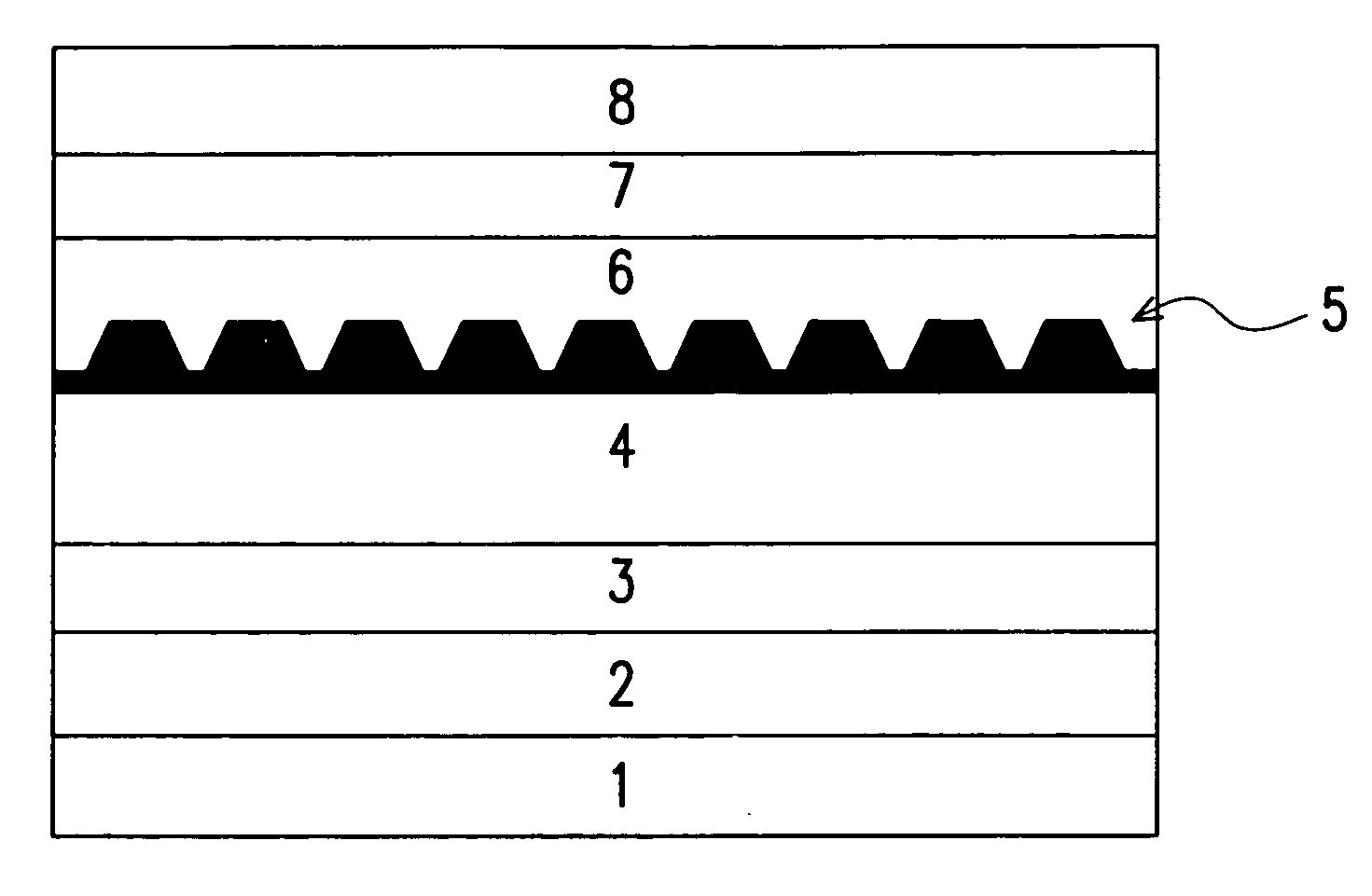
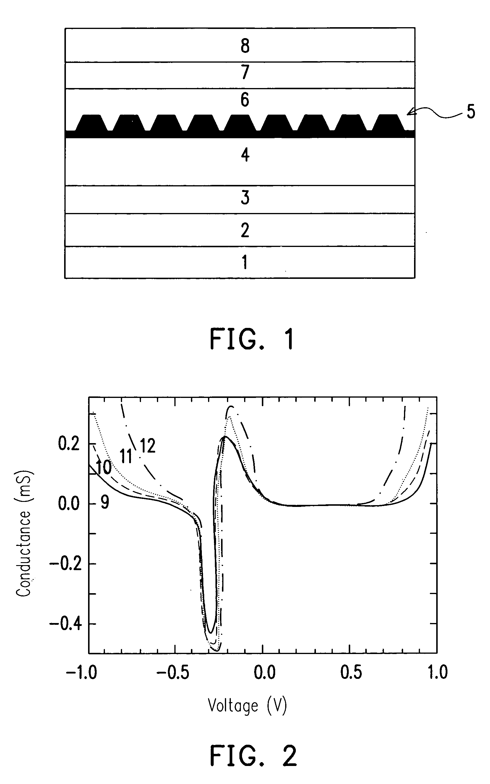
[0020] The molecular beam epitaxy (MBE) or the metal-organic vapor phase epitaxy (MOCVD) technique is used as a preferred process for fabricating the device of the present invention in an epitaxial equipment. The process includes the following steps. First, a GaAs substrate sealed in the nitrogen package is opened and put into the epitaxy machine mentioned above, and the machine temperature is increased to about 580˜630° C., such that the poorly bonded layer and the native oxide layer can be removed from the surface of the substrate. Next, the temperature is fixed on 580˜610° C. to grow and form a buffer layer that is also used as a bottom semiconductor electron injection layer. Then, the growth temperature is reduced to 470˜530° C., so as to form a bottom semiconductor barrier layer defined by the one of periodic double-barriers. Then, the growth temperature is maintained on 470˜530° C., so as to grow a periodic bottom semiconductor spacer layer and a periodic quantum-dot array lay...


PUM


Abstract

A quantum-dot resonant-tunneling device apparatus is provided. The quantum-dot resonant-tunneling device apparatus includes a pair of top-and-down N-type electron injection layers and a pair of quantum-dot layers sandwiched with at least a period of double-barrier. The pair of top-and-down N-type electron injection layers is provided with an adequate positive or negative electric field which leads to electronic resonant-tunneling transportation in the quantum-dot layers mentioned above. In addition, once the electrons are tunneling transported in the device, the device serves as a negative resistance device. The device does not only provide bipolar negative resistance capability and a superior temperature stability within a very wide temperature range, but also operates well under room temperature.

Description

CROSS-REFERENCE TO RELATED APPLICATION [0001] This application claims the priority benefit of Taiwan application serial no. 94113583, filed on Apr. 28, 2005. All disclosure of the Taiwan application is incorporated herein by reference. BACKGROUND OF THE INVENTION [0002] 1. Field of the Invention [0003] The present invention relates to an electronic device apparatus, and more particularly, to a resonant-tunneling quantum-dot semiconductor device. In such device, the resonant-tunneling effect occurs in the electron transportation via quantum dots due to the three dimensional energy band confined enhancement. Accordingly, the device serves as a negative resistance device in the macro electrical characteristics, high temperature-stability and can be operated at room temperature. [0004] 2. Description of the Related Art [0005] In the conventional electronic devices such as High Electron Mobility Transistor (HEMT) or Metal Oxide Semiconductor Field Effect Transistor (MOSFET), the electron...

Claims


Application Information

Patent Timeline
Patent Type & Authority Applications(United States)
IPC IPC(8): H01L29/06
CPCH01L29/882B82Y10/00
Inventor TANG, SHIANG-FENGCHIANG, CHENG-DERYANG, SAN-TERUO, JIUNN-JYEYEN, SHUN-LUNG
Owner NAT CHUNG SHAN INST SCI & TECH
Why Eureka
Try Eureka