

Method for manufacturing semiconductor device
a manufacturing method and semiconductor technology, applied in the direction of semiconductor devices, basic electric elements, electrical appliances, etc., can solve the problems of increased cost, difficult to reuse a substrate, and affect the property of transistors, and achieve the effect of low cost and high reliability
- Summary
- Abstract
- Description
- Claims
- Application Information
AI Technical Summary
Benefits of technology
Problems solved by technology
Method used
Image

Examples
embodiment mode 1
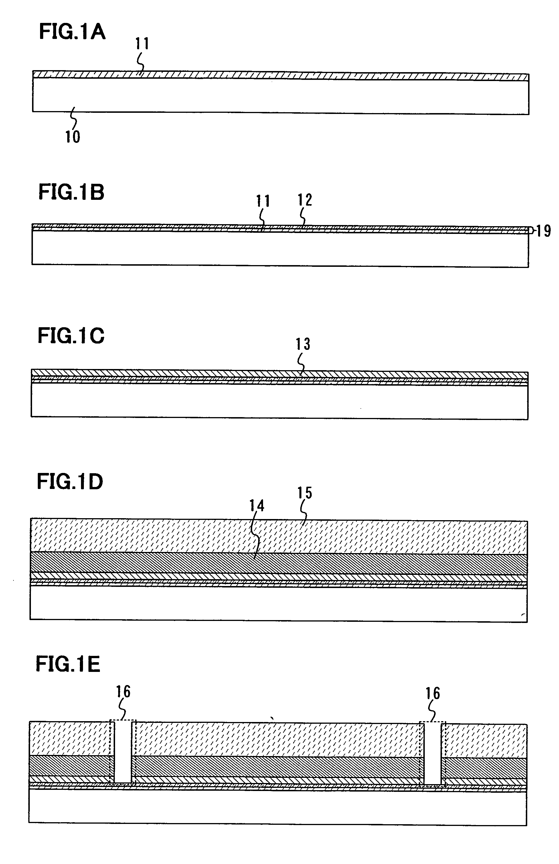
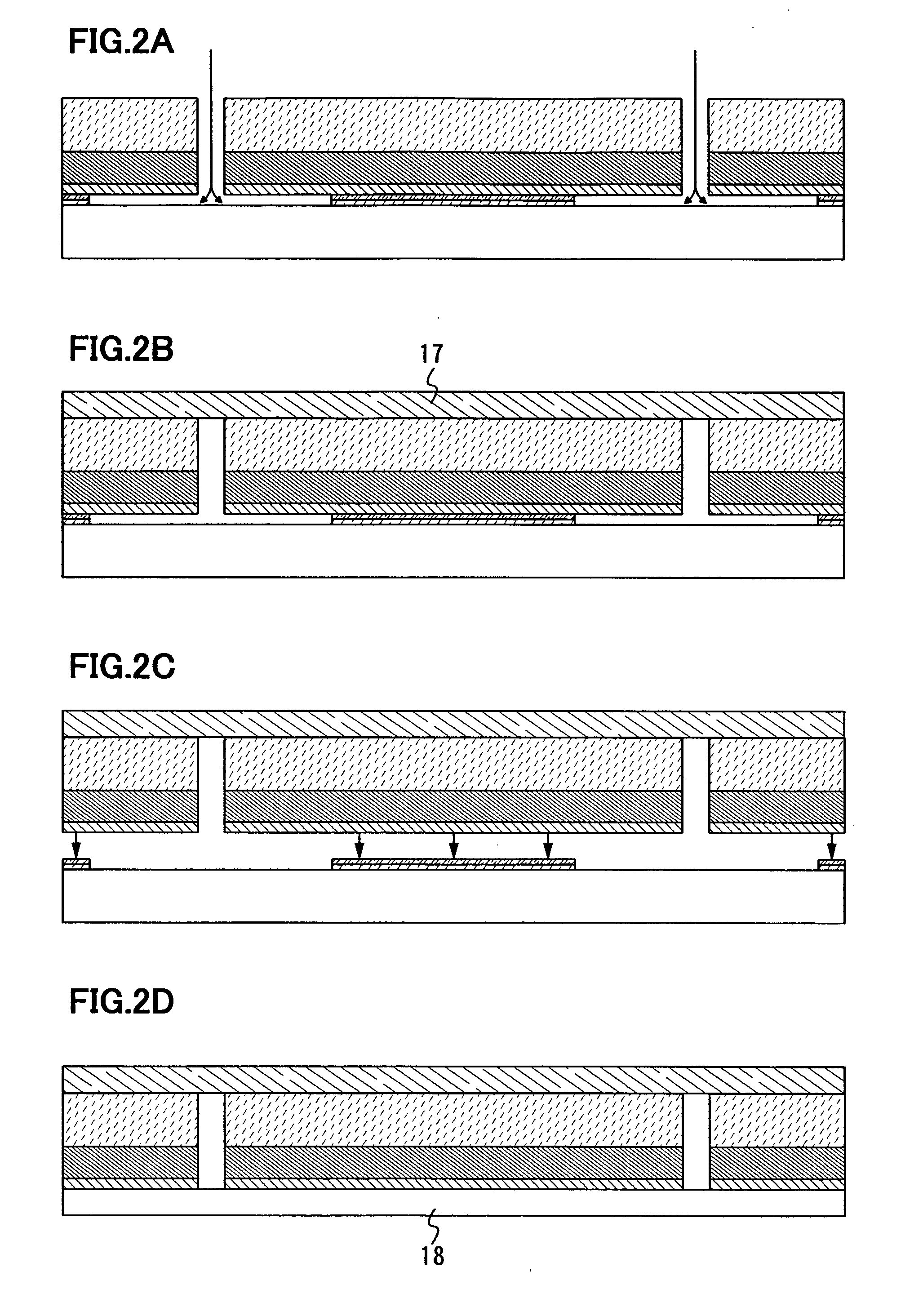
[0046] In this embodiment mode, one constitution example of a method for manufacturing a semiconductor device according to the present invention will be explained with reference to drawings.
[0047] First, a metal film 11 is formed over a surface of a substrate 10 (FIG. 1A). The metal film 11 may be formed in a single layer or a plurality of layers to be stacked. Note that an insulating film may be provided over the substrate 10 before forming the metal film 11. It is preferable to provide an insulating film between the substrate 10 and the metal film 11 particularly when the contamination from the substrate may occur.
[0048] As for the substrate 10, a glass substrate, or a heat resistant plastic substrate or the like that can withstand heat treatment in a manufacturing process of a semiconductor device is preferably used. There is no limitation to the area or shape of the substrate in using such a substrate, and thus, a rectangular substrate having one side of 1 meter or more, for e...
embodiment mode 2
[0078] In this embodiment mode, a method for manufacturing a semiconductor device different from that in the above embodiment mode in forming a peeling layer will be explained with reference to drawings.
[0079] First, a peeling layer formed of a metal oxide film 21 is formed over a surface of a substrate 10 (FIG. 3). The metal oxide film 21 may be formed in a single layer or a plurality of layers to be stacked. Note that an insulating film may be provided over the substrate 10 before forming the metal oxide film 21. It is preferable to provide an insulating film between the substrate 10 and the metal oxide film 21 particularly when the contamination from the substrate may occur.
[0080] As the metal oxide film 21, an oxide of one or more of metal elements such as tungsten (W), molybdenum (Mo), titanium (Ti), tantalum (Ta), niobium (Nb), nickel (Ni), cobalt (Co), zirconium (Zr), zinc (Zn), ruthenium (Ru), rhodium (Rh), palladium (Pd), osmium (Os), and iridium (Ir), or an oxide film of...
embodiment mode 3
[0085] In this embodiment mode, a case of continuously forming an amorphous semiconductor film of a thin film transistor including a peeling layer, an insulating film (a base film), and an element layer over a glass substrate will be explained with reference to drawings.
[0086] An example of an apparatus having a plurality of chambers (multichamber) is shown in FIG. 4. Note that FIG. 4 is a top view of one structural example of an apparatus (continuous film forming system) shown in this embodiment mode.
[0087] The apparatus shown in FIG. 4 has a first chamber 111, a second chamber 112, a third chamber 113, and a fourth chamber 114, load lock chambers 110 and 115, and a common chamber 120 each of which has airtightness. Each chamber is provided with a vacuum evacuation pump and an inert gas introduction system.
[0088] The load lock chambers 110 and 115 are chambers for carrying a sample (a substrate to be processed) to a system. The first to fourth chambers are chambers for forming a...
PUM
 Abstract
Description
Claims
Application Information