

Electro-chemical deposition system
- Summary
- Abstract
- Description
- Claims
- Application Information
AI Technical Summary
Benefits of technology
Problems solved by technology
Method used
Image

Examples
Embodiment Construction
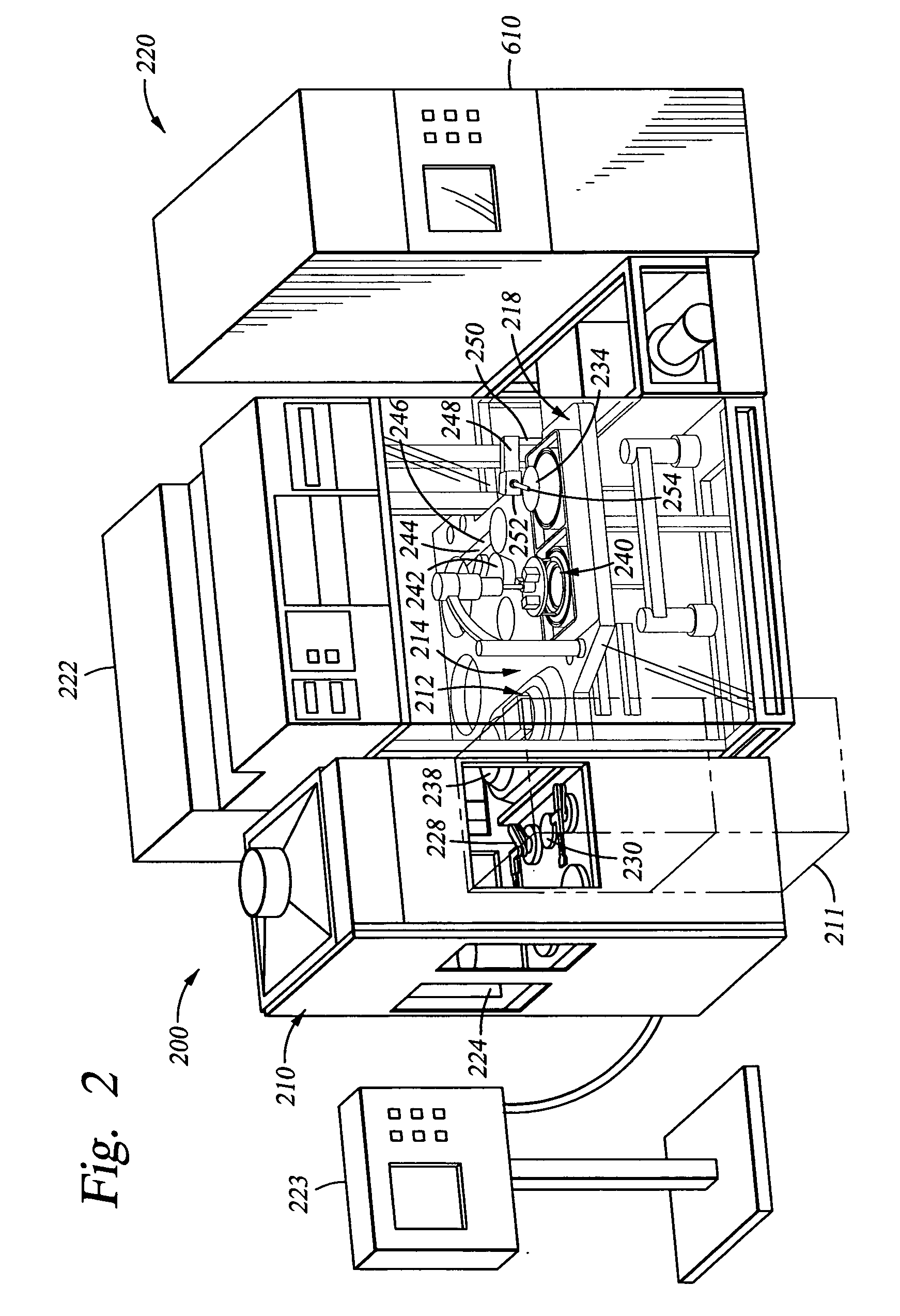
[0053]FIG. 2 is a perspective view of an electroplating system platform 200 of the invention. FIG. 3 is a schematic view of an electroplating system platform 200 of the invention. Referring to both FIGS. 2 and 3, the electroplating system platform 200 generally comprises a loading station 210, a thermal anneal chamber 211, a spin-rinse-dry (SRD) station 212, a mainframe 214, and an electrolyte replenishing system 220. Preferably, the electroplating system platform 200 is enclosed in a clean environment using panels such as plexiglass panels. The mainframe 214 generally comprises a mainframe transfer station 216 and a plurality of processing stations 218. Each processing station 218 includes one or more processing cells 240. An electrolyte replenishing system 220 is positioned adjacent the electroplating system platform 200 and connected to the process cells 240 individually to circulate electrolyte used for the electroplating process. The electroplating system platform 200 also incl...
PUM
| Property | Measurement | Unit |
|---|---|---|
| Pressure | aaaaa | aaaaa |
| Volume | aaaaa | aaaaa |
| Vacuum | aaaaa | aaaaa |
Abstract
Description
Claims
Application Information