Current-matching variable gain amplifier

a variable gain amplifier and amplifier technology, applied in differential amplifiers, amplifier details, amplifier control details, etc., can solve problems such as difficult to solve, power wastage at high gain mode, and the size of transistors cannot be easily matched, so as to achieve a simple circuit and reduce power wastage

Active Publication Date: 2006-11-23
MICROCHIP TECH INC
View PDF17 Cites 14 Cited by
  • Summary
  • Abstract
  • Description
  • Claims
  • Application Information

AI Technical Summary

Benefits of technology

[0008] An object of the present invention is to provide a current-matching variable gain amplifier, which has simpler circuit, do...

Problems solved by technology

But the problem is, in order to achieve an accurate gain value, the sizes of the NMOS transistors 211 and 213 must be appropriately matched, and this problem is not easy t...

Method used


Image

  • Current-matching variable gain amplifier
  • Current-matching variable gain amplifier
  • Current-matching variable gain amplifier

Examples


Embodiment Construction

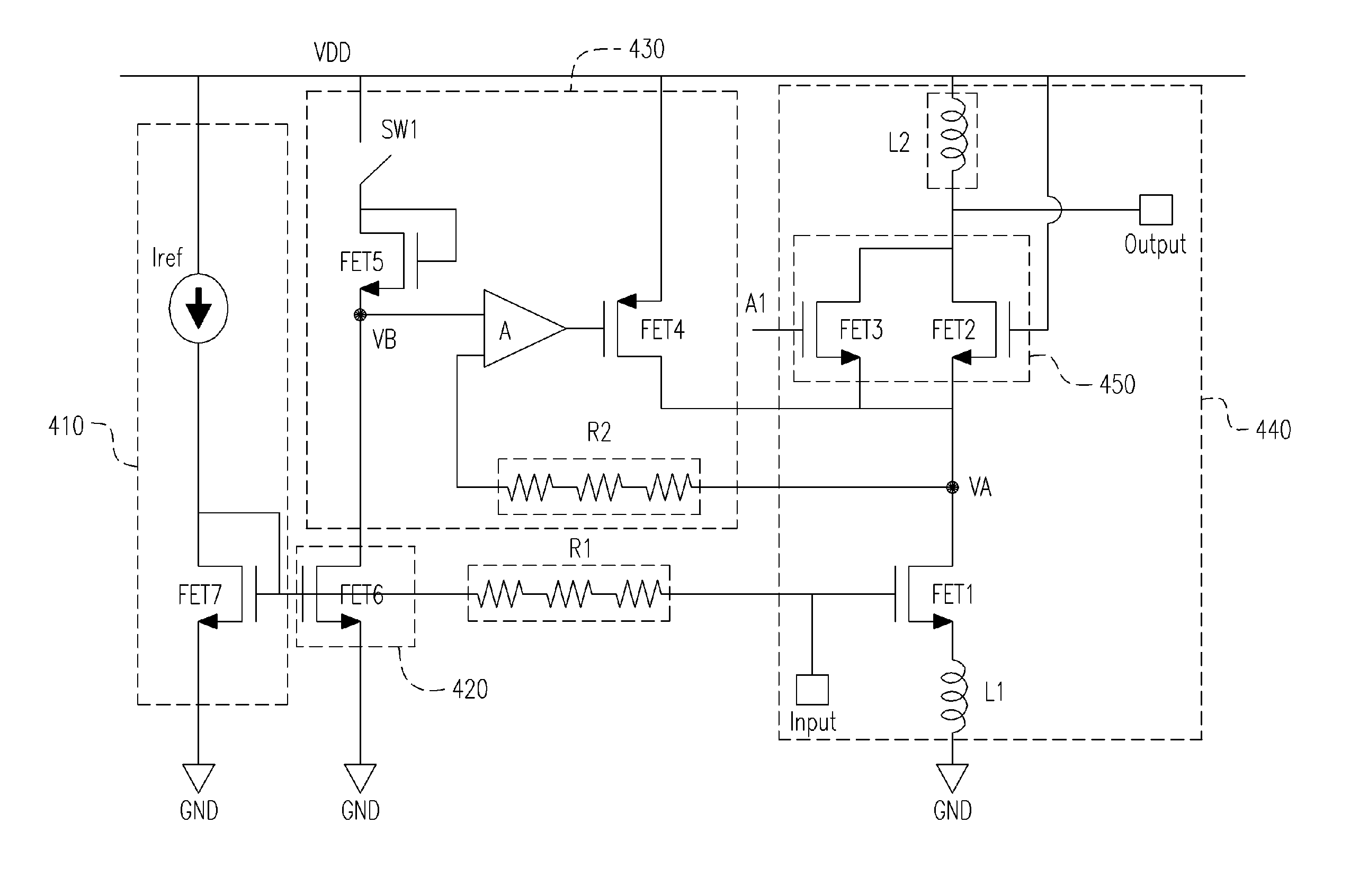
[0023]FIG. 3 is a schematic drawing of a current-matching variable gain amplifier according to an embodiment of the present invention. The amplifier shown in FIG. 3 comprises a reference current source 410, a cascode amplifier 440, a matching circuit 430, a control circuit 420 and a blocking circuit R1.

[0024] The function of the reference current source 410 is to supply a reference current by the current source Iref, which is equal to the left side of the current mirror.

[0025] In according to the reference current of the reference current source 410, the cascode amplifier 440 receives an input signal from an input terminal, amplifies and further outputs the signal at an output terminal as an output signal. Although the illustrated embodiment in FIG. 3 is a single-sided cascode amplifier with only one cascode amplifier 440, the present invention is not limited to only one cascode simplifier. In other embodiments, two or more cascode amplifiers can be included.

[0026] The cascode am...


PUM


Abstract

A current-matching variable gain amplifier is provided. The amplifier comprises a reference current source, at least one cascode amplifier, a matching circuit, a control circuit, and at least one first blocking circuit. The reference current source provides a reference current. Each of the cascode amplifiers amplifies an input signal according to the reference current. The matching circuit equalizes the voltage level at a first node in each cascode amplifier and the voltage level at a second node in the matching circuit. The matching circuit also equalizes the current of a main MOSFET of each cascode amplifier and the current of a first MOSFET of the matching circuit. The control circuit controls the current of the first MOSFET of the matching circuit. Each of the first blocking circuit(s) corresponds with the cascode amplifier, and is coupled between the reference current source and the corresponding cascode amplifier, for blocking RF signals.

Description

BACKGROUND OF THE INVENTION [0001] 1. Field of the Invention [0002] This invention generally relates to a variable gain amplifier, and especially to a current-matching variable gain amplifier. [0003] 2. Description of Related Art [0004] Following the rapid development in radio communication field, a lot of people have been engaged in the research of variable gain amplifier. Up to now, though many solutions have been introduced, there is still room for improvement. [0005]FIG. 1 is a schematic circuit drawing of a variable gain amplifier according to an U.S. patent 2003 / 0181181. Wherein, Input is an input terminal, Output is an output terminal, and Inductor 202 is a load of the amplifier circuit. The amplifier utilizes a control signal 201 to turn on or turn off n-channel metal oxide semiconductor field effect transistor (i.e. NMOSFET, as NMOS transistor hereinafter) 211 and 212, for changing a current passing through the inductor 202, and switching between two gains. At a high gain m...

Claims


Application Information

Patent Timeline
IPC IPC(8): H03F3/45
CPCH03F1/223H03G1/0088H03F3/193
Inventor CHIANG, MING-CHOU
Owner MICROCHIP TECH INC
Why Eureka
Try Eureka