Semiconductor optical device and module using the same

a technology of semiconductor lasers and optical devices, applied in semiconductor lasers, laser optical resonator construction, laser details, etc., can solve the problems of difficult suppression of inability to completely suppress scattering and reflection of light waves at this site, and inability to use structures in practical use. , to achieve the effect of reducing light scattering and light reflection, high output power, and high reliability of single lateral mode laser diodes

Inactive Publication Date: 2006-12-07
OPNEXT JAPAN INC
View PDF8 Cites 31 Cited by
  • Summary
  • Abstract
  • Description
  • Claims
  • Application Information

AI Technical Summary

Benefits of technology

[0020] In order to solve the above-described problems, the present inventors have designed a taper MMI structure as described below. That is, in the waveguide structure of the MMI laser diode, a taper waveguide is intentionally inserted between the single mode waveguide and the multimode waveguide. As a result, light scattering and light reflection are reduced at this site as well as a primary laser vertical resonance mode is prevented from being unstable when an uncontrollable slight reflected light returns again to the inside of the laser resonator. Further, the present inventors have designed a laser diode structure as described below. That is, in the waveguide structure of the MMI laser diode, a single mode waveguide is used as a passive waveguide. As a result, the manufactured laser diode structure is suitable particularly for CD laser diodes or DVD laser diodes, in which the optical power density has a significant effect on device reliability. When these units are used individually or in combination thereof, a high output power and high reliability of the single lateral mode laser diode can be simultaneously realized. Further, the present inventors have found the following fact. That is, in the case of incorporating an optical reflecting mirror formed using a grating into a single mode waveguide, even when an operating temperature of devices changes, conditions hardly vary where a loss of the MMI waveguide is reduced. Based on this finding, the MMI laser diode having more excellent characteristics is realized.
[0021] Incidentally, in this MMI laser diode, high optical output power can be realized by a short laser resonator length. Therefore, when this laser diode is used, a variety of new high power laser diodes are realized. For example, in the case of monolithically integrating the MMI DVD laser diode and the CD laser diode, when using a conventional CD laser resonator length of about 1300 μm or less, a high output power of the MMI DVD laser diode can be realized. Further, also in the case of integrating a short resonator-type laser diode into a cheaper CD package, high output power of the laser diode can be attained without impairing a high power property.
[0022] According to the present invention, in the case of monolithically integrating the MMI DVD laser diode and the CD laser diode, when a conventional CD laser resonator length of about 1300 μm or less is used, high output power of the MMI DVD laser diode can be realized. Further, also in the case of integrating a short resonator-type laser diode into an inexpensive CD package, high output power of the laser diode can be attained without impairing a high power property.

Problems solved by technology

However, these structures have the following problems.
Therefore, it is still the case where the structures are not always in practical use in a wide range.
A first problem is difficulty of suppressing scattering and reflection of light waves caused by a rapid change of a waveguide width at the border between a multimode waveguide region and a single mode waveguide region.
It is impossible to completely suppress the scattering and reflection of light waves at this site.
As a result, an oscillation mode becomes unstable and therefore a structure capable of automatically preventing this problem is required.
A second problem is a difference between optical power density in the multimode waveguide region and that in the single mode waveguide region.
That is, a high power operation of the laser diode is limited due to reliability deterioration accompanying a crystal breakdown in the single mode waveguide region or due to an optical non-linear phenomenon caused by, for example, lateral hole burning.
As a result, there arise big problems in that performance of the CD laser diode is deteriorated as well as an increase in substrate area leads to economical inefficiency.

Method used


Image

  • Semiconductor optical device and module using the same
  • Semiconductor optical device and module using the same
  • Semiconductor optical device and module using the same

Examples


first embodiment

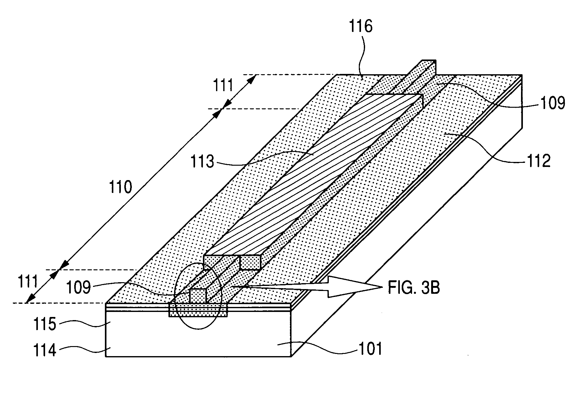
[0038]FIG. 3A is a perspective view of a 650-nm range high power DVD laser diode structure according to a first embodiment of the present invention, FIG. 3B is its partial enlarged lateral view and FIG. 4 is its top view.

[0039] On an n-type angled GaAs substrate 101 offset at 10 deg. from a (100) surface orientation, an n-type GaAs buffer layer 102 with a film thickness of 0.5 μm, an n-type AlGaInP cladding layer 103, a multi-quantum-well active layer 104, a first p-type AlGaInP cladding layer 105 with a film thickness of 0.05 μm, a p-type GaInP etching stop layer 106 with a film thickness of 5 nm, a second p-type AlGaInP cladding layer 107 with a film thickness of 1.5 μm, and a p+ type GaAs contact layer 108 with a film thickness of 0.2 μm are sequentially epitaxially grown by metalorganic vapor phase epitaxy (MOVPE). The Multi-quantum-well active layer 104 comprises three undoped compression strain GaInP quantum-well layers with a film thickness of 5 nm, four tensile strain AlGaI...

second embodiment

[0042]FIGS. 6A, 6B and 7 are diagrams showing a structure of a semiconductor laser diode according to a second embodiment of the present invention. The second embodiment differs from the first embodiment in a structure of the MMI waveguide; however, the semiconductor laminated structure of the semiconductor laser diode in the second embodiment is the same as that in the first embodiment. FIG. 6A is a perspective view showing a structure of a 650 nm range high power DVD laser diode. FIG. 6B is its partial enlarged view and FIG. 7 is its top view.

[0043] As shown in FIG. 7, the present embodiment provides a taper MMI structure as described below. That is, in the waveguide structure of the MMI laser diode, a taper waveguide 150 is intentionally inserted between a single mode waveguide and a multimode waveguide. As a result, light scattering and light reflection are reduced at this site as well as an original laser vertical resonance mode is prevented from being unstable when an uncontr...

third embodiment

[0049]FIG. 11 is a perspective view of a monolithic two-wavelength laser diode manufactured by monolithically integrating a 650-nm range high power DVD laser diode 201 and a 780-nm range high power CD laser diode 202 according to a third embodiment of the present invention. Herein, the DVD laser diode has the same structure as the taper MMI laser diode shown in the second embodiment and has a resonator length of 1300 μm. On the other hand, the CD laser diode is a known AlGaAs buried ridge type laser diode and has a normal single-mode-waveguide structure. At a temperature of 80° C., the DVD laser diode attains a kink-free maximum optical output power of 350 mW and the CD laser diode attains a kink-free maximum optical output power of 250 mW. These values are suited to DVD double-layer eightfold-speed writing and CD single-layer forty eight-fold speed writing.


PUM


Abstract

A semiconductor laser device capable of providing high output power operation is provided which has a structure in which high output power and kink suppression can be simultaneously attained as well as these characteristics can be realized by a short chip length. In a waveguide structure of an MMI laser diode, a taper waveguide is intentionally inserted between a single mode waveguide and a multimode waveguide, and further, a single mode waveguide is used as a passive waveguide. These individual units or combination thereof can solve the above-described problems.

Description

CLAIM OF PRIORITY [0001] The present application claims priority from Japanese application JP 2005-163576, filed on Jun. 3, 2005, the content of which is hereby incorporated by reference into this application. BACKGROUND OF THE INVENTION [0002] 1. Field of the Invention [0003] The present invention relates to a semiconductor optical device and a module using the same technologies. More specifically, the present invention relates to a light source of a semiconductor optical device that stably operates at high optical output power suitable for an information processing terminal or for optical communication. [0004] 2. Description of the Related Arts [0005] A technical difficulty in realizing a high power semiconductor laser diode is a permanent problem irrespective of application fields. According to respective application fields, research and development of high power laser diodes with various wavebands are still performed energetically. These high power semiconductor laser diodes can...

Claims


Application Information

Patent Timeline
Patent Type & Authority Applications(United States)
IPC IPC(8): H01S5/00H01S5/12
CPCB82Y20/00H01S5/02212H01S5/1014H01S5/1039H01S5/12H01S5/4087H01S5/162H01S5/22H01S5/34326H01S5/3436H01S5/4031H01S5/1237
Inventor AOKI, MASAHIRONOMOTO, ETSUKO
Owner OPNEXT JAPAN INC
Why Eureka
Try Eureka