Method for encapsulating electronic devices and a sealing assembly for the electronic devices

a technology of which is applied in the field of encapsulating electronic devices and sealing assemblies for electronic devices, can solve the problems of low work function metals, reduced performance, and sensitive organic electronic devices, and achieves the effects of reducing process time and cost, reducing device thickness, and simplifying the encapsulation process

Inactive Publication Date: 2006-12-21
EI DU PONT DE NEMOURS & CO
View PDF62 Cites 94 Cited by
  • Summary
  • Abstract
  • Description
  • Claims
  • Application Information

AI Technical Summary

Benefits of technology

[0104] The present methods for adhering a getter to a substrate are completely independent of the manufacturing of the device. Since heat treatment of the getter is independent of the device, no special consideration of the sensitivities of the device need be taken in manufacturing of the getter and no special consideration of the sensitivities of the getter (i.e., deactivation) need be taken in manufacturing of the device until the getter is encapsulated along with the device into the enclosure.
[0105] The use of spacers in the epoxy allows for the use of thin flat glass for both the substrate and the lid, greatly reducing the thickness of the device when compared to a cavity-type lid. In addition, this embodiment simplifies the encapsulation process, reducing process time and costs, and even reducing the amount of time need...

Problems solved by technology

Organic electronic devices are sensitive to, and have decreased performance, when critical components are exposed to undesirable contaminants, including moisture and other contaminant gases, such as oxygen, hydrogen, and organic gases.
Unfortunately, low work function metals such as calcium, barium and strontium typically react with oxygen and form water vapor.
These reactions destroy their required low work function property.
Manufacture of organic electronic devices presents certain process limitations to the use of getters.
Absorbent getters are inherently moisture sensitive and the absorption reaction is not reversible, requiring manufacture in a lo...

Method used


Image

  • Method for encapsulating electronic devices and a sealing assembly for the electronic devices
  • Method for encapsulating electronic devices and a sealing assembly for the electronic devices
  • Method for encapsulating electronic devices and a sealing assembly for the electronic devices

Examples


example 1

[0109] This example illustrates the present invention applying the getter composition. The getter composition was a liquid dispersion of particles of a zeolite-based molecular sieve and glass frit in an organic liquid medium. The dispersion comprised the following ingredients by wt % of total dispersion:

[0110] Inorganic Components:

Zeolite-based molecular sieve (13x-typed powder)54.1Glass frit5.4

[0111] Organic Components:

surfactant1.1ethylcellulose resin1.0Texanol solvent (ester alcohol)38.4%

[0112] The composition of the glass frit in wt % (dry) was as follows:

SiO2Al2O3B2O3CaOZnOBi2O37.112.138.380.5312.0369.82

example 2

[0113] This example illustrates making and performance of method of applying the getter composition of the present invention. A slurry of 0.75 tablets of unfired DESIWAFER 300 / 20 zeolite-clay material in 1 ml of water was dispersed in water to make a 200 ml dispersion. The dispersion was applied to a cavity on a glass lid plate in 0.5 ml aliquots by hand using a syringe. The getter was solidified by placing in a vacuum oven for 1 hour at 70° C. to remove substantially all of the water. After solidification, the getter layers were then activated and densified by heating the glass lid plates for 2 hours at 500° C. In an environment having less than 10 ppm H2O and O2, the plates with self-attached getter layers were then each assembled into an enclosure holding a polymer light emitting diode device (“PLED”). Control devices were assembled into an enclosure under the same conditions, except that the getter layer was replaced by a fired DESIWAFER tablet (Sud-Chemie) attached to a plate b...

example 3

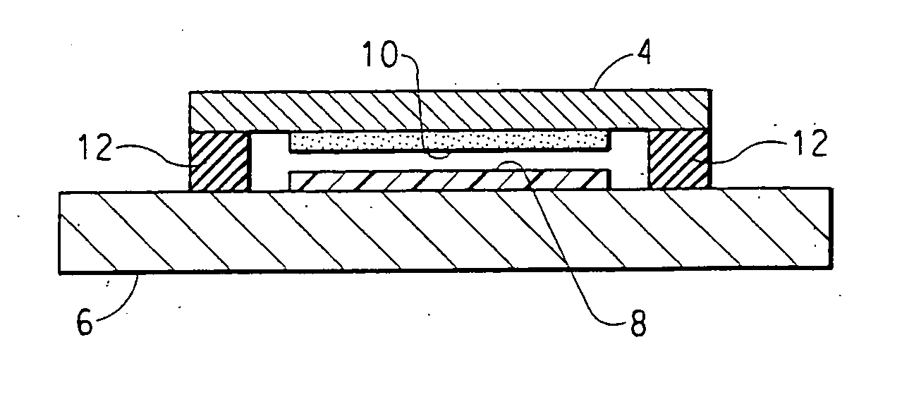
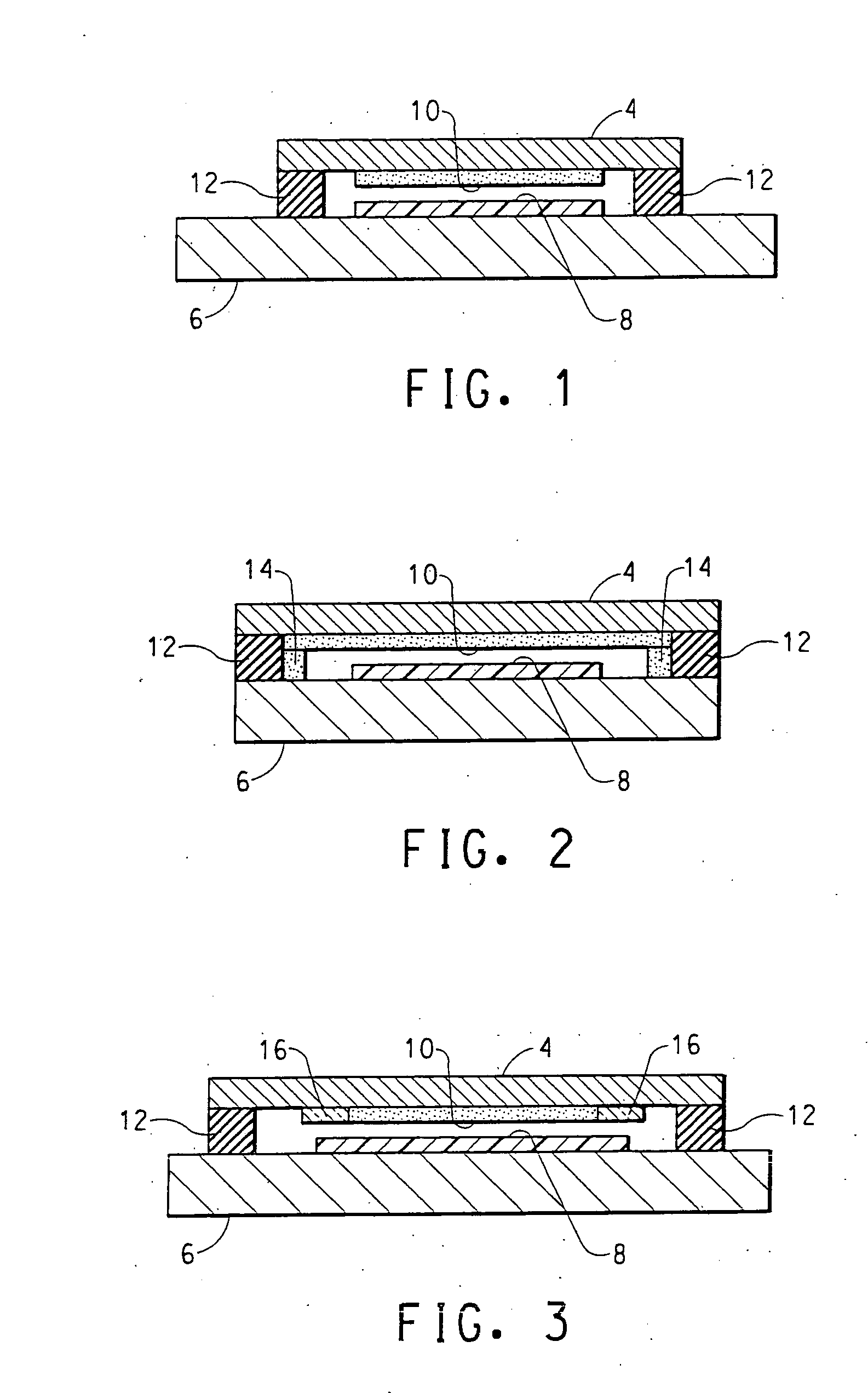
[0114] This example illustrates the use of a sealing composition comprising spacer beads dispersed in epoxy to provide the separation between two flat plates in an organic electronic device. This example further illustrates the use of a getter ledge for sealing under reduced pressure.

[0115] An approximately 30 micron getter layer was formed on an approximately 0.3 mm thickness flat glass lid using the method as described in Example 2. The getter layer was formed in a pattern to provide a ledge around the perimeter of a device. An OLED was formed on an approximately 0.3 mm thickness flat glass substrate, and an epoxy containing 2% by volume of 50 micron glass frit beads was used to seal the lid to the OLED. The epoxy was applied to the exterior of the getter ledge and the device was sealed under vacuum. The resulting device had a thickness of approximately 0.64 mm.


PUM

PropertyMeasurementUnit
Temperatureaaaaaaaaaa
Timeaaaaaaaaaa

Abstract

A method for sealing an electronic device includes providing an electronic device on a substrate, providing a lid, activating a getter material in an environment substantially free of contaminants, applying a sealing material to at least a portion of the lid, and attaching the substrate and the lid in an inert environment. The time elapsed between activating the getter material and attaching the substrate and the lid is less than 20 minutes. A sealing assembly for an electronic device includes an activation tool for activating a getter material, a dispensing tool for dispensing a sealing material, and an encapsulation tool for sealing the electronic device. The sealing assembly is in an environment substantially free of contaminants.

Description

CROSS REFERENCE TO RELATED APPLICATIONS [0001] This is a Continuation-In-Part of application Ser. No. 10 / 984,451, filed on Nov. 9, 2004, which claims priority to Provisional Application Ser. No. 60 / 519,139, filed on Nov. 12, 2003, both of which are incorporated herein by reference in their entirety.BACKGROUND INFORMATION [0002] 1. Field of the Disclosure [0003] This disclosure relates in general to a method for encapsulating electronic devices and a sealing assembly for the electronic devices. [0004] 2. Description of the Related Art [0005] Organic electronic devices are sensitive to, and have decreased performance, when critical components are exposed to undesirable contaminants, including moisture and other contaminant gases, such as oxygen, hydrogen, and organic gases. For example, the relatively low work function metals, such as barium or calcium, are often used as the cathode material in electronic organic devices for device performance reasons. Unfortunately, low work function...

Claims


Application Information

Patent Timeline
IPC IPC(8): B05D5/12C23C16/00B32B37/12
CPCC03C3/066C03C8/04C03C8/24C03C27/06C03C27/10H01L23/26H01L51/448H01L2924/0002H01L51/5237H01L2924/09701H01L2924/12044Y02E10/549H01L2924/00Y02P70/50H10K30/88H10K50/8428H10K50/846H10K50/8426H10K50/87H10K2102/361
Inventor TREMEL, JAMES DANIELHUBERT, MATTHEW DEWEY
Owner EI DU PONT DE NEMOURS & CO
Why Eureka
Try Eureka