A Stretchable Form of Single Crystal Silicon for High Performance Electronics on Rubber Substrates

a technology of electronics and single crystal silicon, which is applied in the direction of final product manufacturing, semiconductor/solid-state device details, sustainable manufacturing/processing, etc., can solve the problems of inability to bind to most plastic materials, inability to bind to most inorganic semiconductors in convenient solvents, and well-developed methods of making conventional silicon-based electronic devices. exhibiting good electronic performance, the effect of significant elongation, flexing and bending

Active Publication Date: 2006-12-21
THE BOARD OF TRUSTEES OF THE UNIV OF ILLINOIS
View PDF65 Cites 275 Cited by
  • Summary
  • Abstract
  • Description
  • Claims
  • Application Information

AI Technical Summary

Benefits of technology

[0012] The present invention provides stretchable semiconductors and stretchable electronic devices, device components and circuits. As used herein, the term “stretchable” refers to materials, structures, devices and device components capable of withstanding strain without fracturing or mechanical failure. Stretchable semiconductors and electronic devices of the present invention are extensible and, thus, are...

Problems solved by technology

Second, the inherent flexibility of these substrate materials allows them to be integrated into many shapes providing for a large number of useful device configurations not possible with brittle conventional silicon based electronic devices.
The design and fabrication of flexible electronic devices exhibiting good electronic performance, however, present a number of significant challenges.
First, the well developed methods of making conventional silicon based electronic devices are incompatible with most plastic materials.
In addition, most inorganic semiconductors are not intrinsically soluble in convenient solvents that would allow for solution based processing and delivery.
Second, although many amorphous silicon, organic or hybrid organic-inorganic semiconductors are compatible with incorporation into plastic substrates and can be processed at relatively low temperatures, these materials do not have electronic properties capable of providing integrated electronic devices capable of good electronic performance.
As a result of these limitations, flexible electronic devices are presently limited to specific applications not requiring high performance, such as use in switching elements for active matrix flat panel displays with non-emissive pixels and in light emitting diodes.
While this class of flexible electronic devices provides enhanced device electronic performance characteristics, use of pulsed laser annealing limits the ease and flexibility of fabrication of such devices, thereby significantly increasing costs.
This device field effect mobility is several orders of magnitude lower than the device field effect mobilities of conventional single crystalline inorganic thin film transistors, and ...

Method used


Image

  • A Stretchable Form of Single Crystal Silicon for High Performance Electronics on Rubber Substrates
  • A Stretchable Form of Single Crystal Silicon for High Performance Electronics on Rubber Substrates
  • A Stretchable Form of Single Crystal Silicon for High Performance Electronics on Rubber Substrates

Examples


example 1

A Stretchable Form of Single Crystal Silicon for High Performance Electronics on Rubber Substrates

[0112] We have produced a stretchable form of silicon that consists of sub-micrometer single crystal elements structured into shapes with microscale periodic, wave-like geometries. When supported by an elastomeric substrate, this ‘wavy’ silicon can be reversibly stretched and compressed to large strains without damaging the silicon. The amplitudes and periods of the waves change to accommodate these deformations, thereby avoiding significant strains in the silicon itself. Dielectrics, patterns of dopants, electrodes and other elements directly integrated with the silicon yield fully formed, high performance ‘wavy’ metal oxide semiconductor field effect transistors, pn diodes and other devices for electronic circuits that can be stretched or compressed to similarly large levels of strain.

[0113] Progress in electronics is driven mainly by efforts to increase circuit operating speeds and...

example 2

Buckled and Wavy Ribbons of GaAs for High-Performance Electronics on Elastomeric Substrates

[0128] Single crystalline GaAs ribbons with thicknesses in the submicron range and well-defined, ‘wavy’ and / or ‘buckled’ geometries are fabricated. The resulting structures, on the surface of or embedded in an elastomeric substrate, exhibit reversible stretchability and compressibility to strains >10%, more than ten times larger than that of GaAs itself. By integrating ohmic and Schottky contacts on these structured GaAs ribbons, high-performance stretchable electronic devices (e.g., metal-semiconductor field-effect transistors) can be achieved. This kind of electronic system can be used alone or in combination with similarly designed silicon, dielectric and / or metal materials to form circuits for applications that demand high frequency operation together with stretchability, extreme flexibility or ability to conform to surfaces with complex curvilinear shapes.

[0129] Performance capabili...

example 3

Two-Dimensional Stretchable Semiconductors

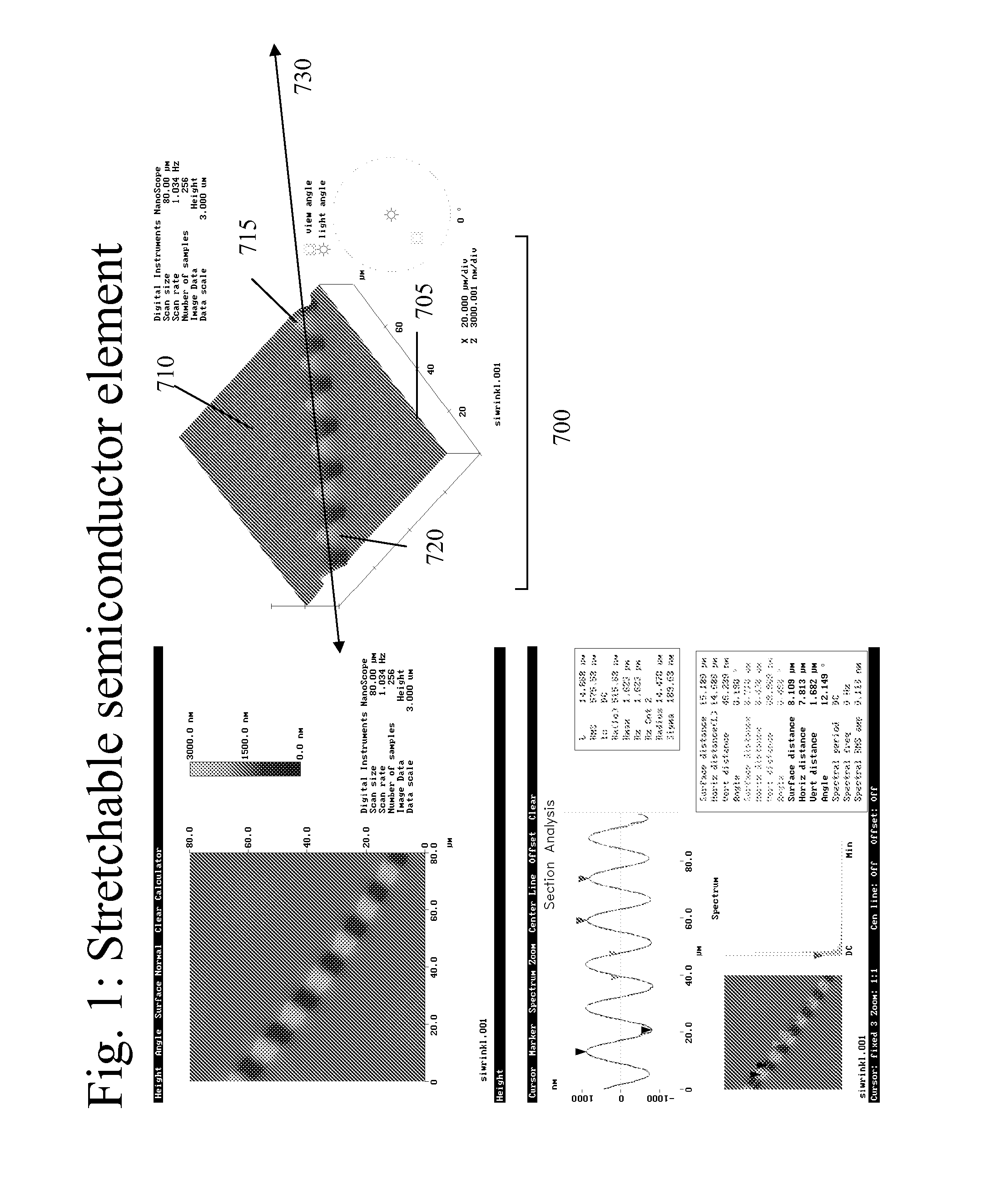
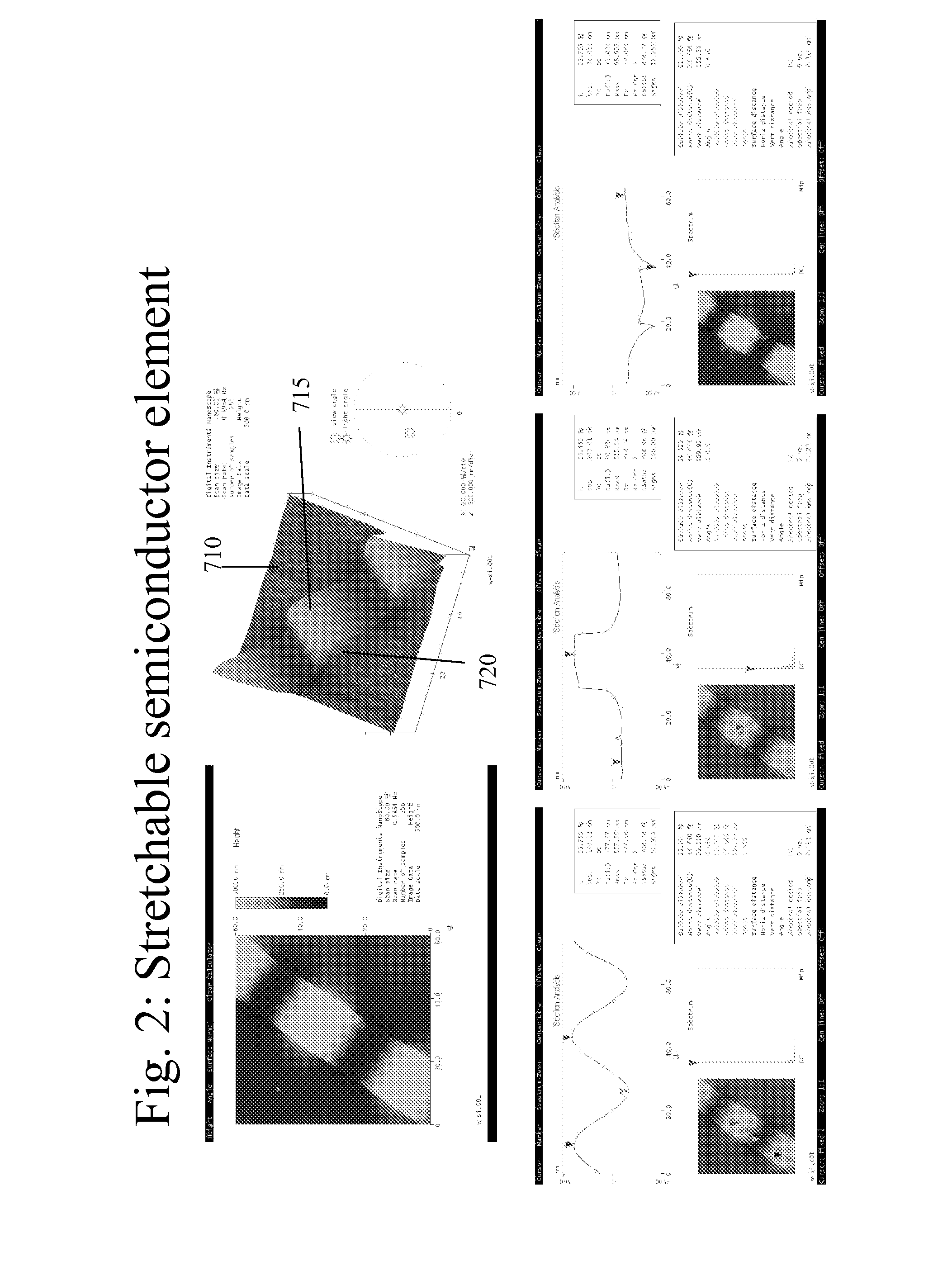
[0141] The present invention provides stretchable semiconductors and stretchable electronic devices capable of stretching, compressing and / or flexing in more than one direction, including directions oriented orthogonal to each other. Stretchable semiconductors and stretchable electronic devices of this aspect of the present invention exhibit good mechanical and electronic properties and / or device performance when stretched and / or compressed in more than one direction.

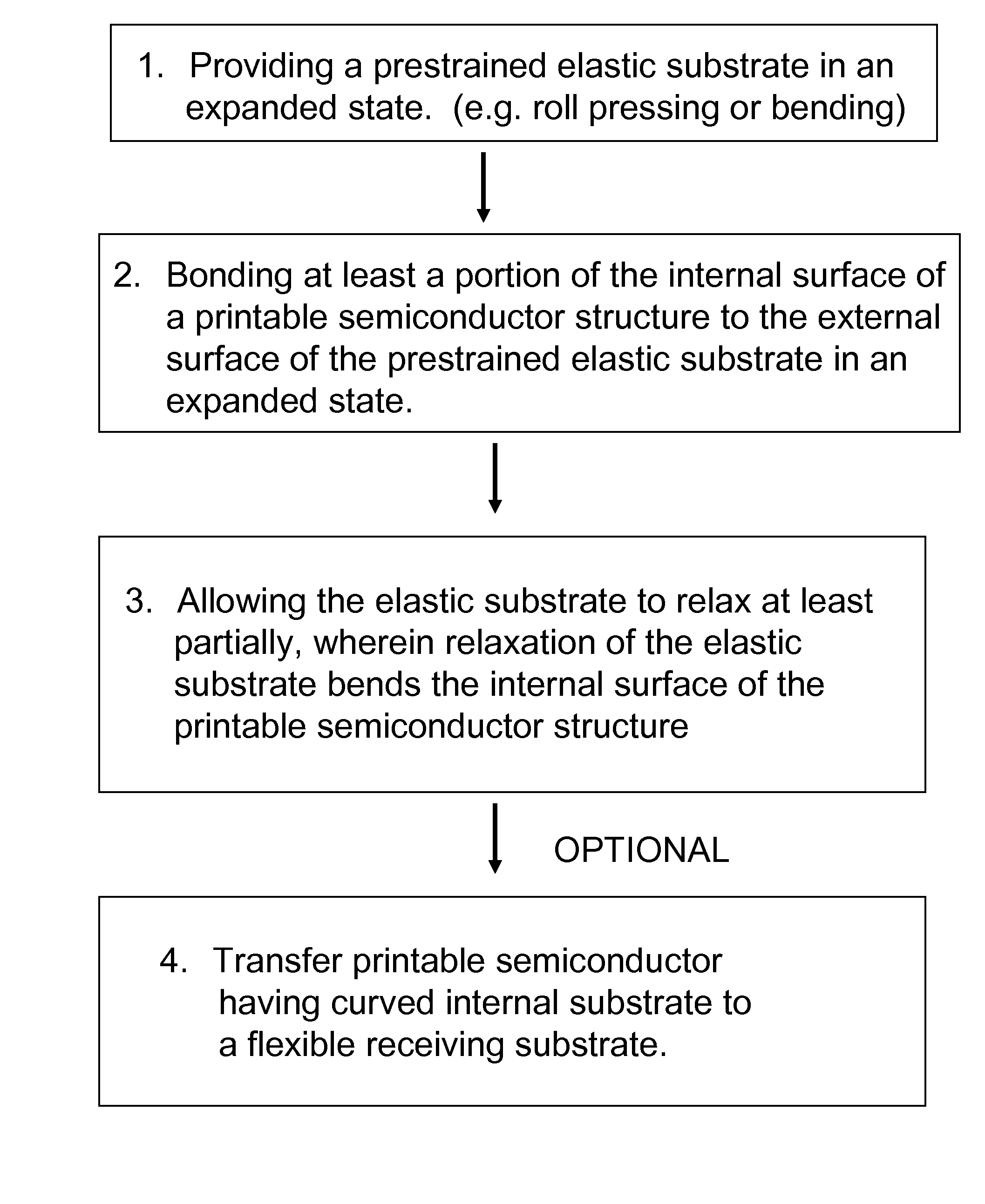
[0142] FIGS. 27A-C provides images at different degrees of magnification of a stretchable silicon semiconductor of the present invention exhibiting stretchability in two dimensions. The stretchable semiconductor shown in FIGS. 27A-B was prepared by pre-straining an elastic substrate via thermal expansion.

[0143] FIGS. 28A-C provide images of three different structural conformations of stretchable semiconductors of the present invention exhibiting stretchability in two di...


PUM


Abstract

The present invention provides stretchable, and optionally printable, semiconductors and electronic circuits capable of providing good performance when stretched, compressed, flexed or otherwise deformed. Stretchable semiconductors and electronic circuits of the present invention preferred for some applications are flexible, in addition to being stretchable, and thus are capable of significant elongation, flexing, bending or other deformation along one or more axes. Further, stretchable semiconductors and electronic circuits of the present invention may be adapted to a wide range of device configurations to provide fully flexible electronic and optoelectronic devices.

Description

CROSS REFERENCE TO RELATED APPLICATIONS [0001] This application is a continuation-in-part of U.S. patent application Ser. No. 11 / 145,542, filed Jun. 2, 2005 and U.S. patent application Ser. No.11 / 145,574, filed Jun. 2, 2005, both of which claim the benefit under 35 U.S.C. 119(e) of U.S. Provisional Patent Application Nos. 60 / 577,077, 60 / 601,061, 60 / 650,305, 60 / 663,391 and 60 / 677,617 filed on Jun. 4, 2004, Aug. 11, 2004, Feb. 4, 2005, Mar. 18, 2005, and May 4, 2005, respectively, and the present application also claims the benefit under 35 U.S.C. 119(e) of U.S. Provisional Patent Application No. 60 / 790,104 filed on Apr. 7, 2006, all of which are hereby incorporated by reference in their entireties to the extent not inconsistent with the disclosure herein.STATEMENT REGARDING FEDERALLY SPONSORED RESEARCH OR DEVELOPMENT [0002] This invention was made, at least in part, with United States governmental support awarded by DARPA-funded AFRL-managed Macroelectronics Program Contract FA8650-0...

Claims


Application Information

Patent Timeline
IPC IPC(8): H01L21/20
CPCB81C2201/0185B82Y10/00H01L21/02628H01L21/6835H01L27/1266H01L29/0665H01L29/0673H01L29/0676H01L29/068H01L29/16H01L29/1602H01L29/1606H01L29/7781H01L29/78603H01L29/78681H01L29/78696H01L31/0392H01L31/18H01L31/1804H01L2221/68368H01L2224/8385H01L2924/01002H01L2924/01003H01L2924/01005H01L2924/0101H01L2924/01011H01L2924/01013H01L2924/01015H01L2924/0102H01L2924/01029H01L2924/0103H01L2924/01032H01L2924/01049H01L2924/01051H01L2924/01074H01L2924/01079H01L2924/01082H01L2924/07802H01L2924/10329H01L2924/10336H01L2924/10349H01L2924/13091H01L2924/3025H01L2924/13063H01L2924/01006H01L2924/01019H01L2924/01023H01L2924/01024H01L2924/01033H01L2924/01067H01L2924/01072H01L29/06H05K1/0277H01L2924/0132H01L21/02422H01L21/02521H01L21/02532H01L21/02546H01L2924/12041H01L23/293H01L29/151H01L29/158Y02E10/547H01L2224/80894H01L24/29H01L24/32H01L24/80H01L2224/291H01L2224/2919H01L27/1285H01L27/1292H01L2924/1461H01L2924/3512H01L2924/00H01L2924/00014H01L2924/12032H01L2924/12042H01L2924/12036H01L31/03925H01L31/03926H01L23/5387H01L2924/0002Y02P70/50H01L29/72H05K1/0283H01L23/3157H01L23/564
Inventor ROGERS, JOHN A.KHANG, DAHL-YOUNGSUN, YUGANG
Owner THE BOARD OF TRUSTEES OF THE UNIV OF ILLINOIS
Why Eureka
Try Eureka