Dye-sensitized solar cell

a solar cell and dye technology, applied in the direction of light-sensitive devices, capacitors, electrolytic capacitors, etc., can solve the problems of high material processing cost and difficulty in developing a dye capable, and achieve the effect of improving light utilization efficiency and light utilization efficiency

Inactive Publication Date: 2006-12-28
NGK SPARK PLUG CO LTD
View PDF7 Cites 38 Cited by
  • Summary
  • Abstract
  • Description
  • Claims
  • Application Information

AI Technical Summary

Benefits of technology

[0005] The present invention has been made according to the above circumstances to provide a dye-sensitized solar cell having two semiconductor electrodes for improved light utilization efficiency, and more spec...

Problems solved by technology

These silicon solar cells show excellent photoelectric conversion efficiency of nearly 20%, but require high energy costs for material processing and have many problems to be addressed such as environmental bu...

Method used


Image

  • Dye-sensitized solar cell
  • Dye-sensitized solar cell
  • Dye-sensitized solar cell

Examples


example 1

[0082] (1) Production of First Laminated Member

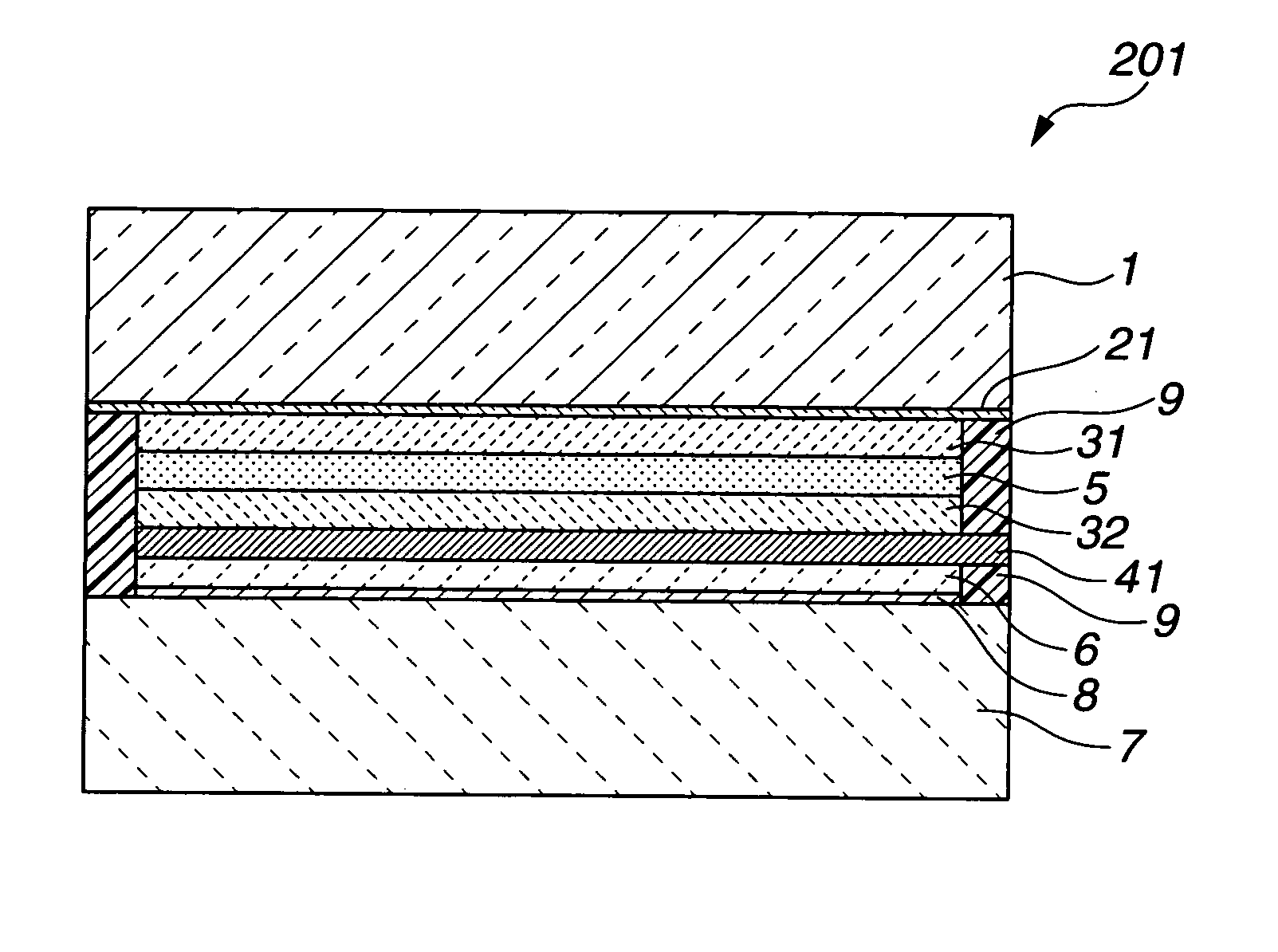
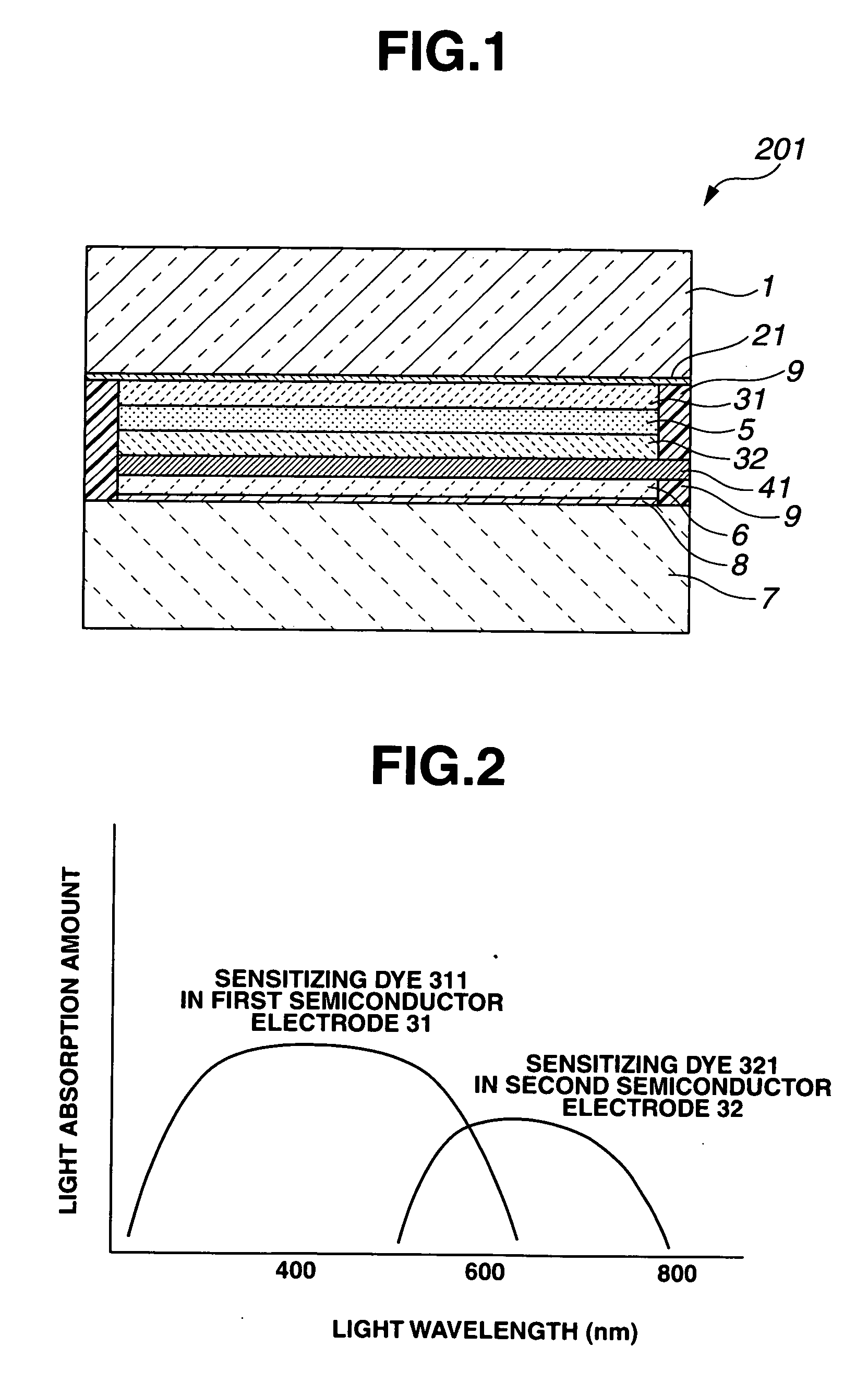
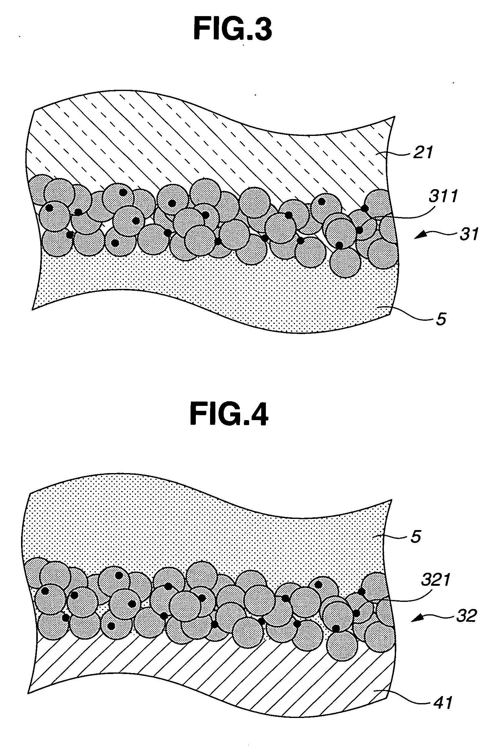
[0083] A glass substrate having a length of 100 mm, a width of 100 mm and a thickness of 1 mm was prepared as a light-transmitting substrate 1. A third collector electrode 43 was formed of tungsten in a grid pattern with a width of 1 mm, a pitch of 10 mm and a thickness of 1 μm on a surface of the substrate 1 by a RF sputtering process. After that, a light-transmitting conductive layer 21 of fluorine-doped tin oxide was formed with a thickness of 500 nm by a RF sputtering process on the surface of the substrate 1 to which the third collector electrode 43 had been applied. An electrode layer (as an electrode body) having a length of 90 mm, a width of 90 mm and a thickness of 20 μm were then formed by applying a paste containing titania particles of 10 to 20 nm in diameter (available under the trade name of “Ti-Nonoxide D / SP” from Solaronix) to a surface of the light-transmitting conductive layer 21 by a screen printing process, drying a...

example 2

[0090] A dye-sensitized solar cell 206 was manufactured in the same manner as in Example 1 except that a second collector electrode 42 of tungsten in sheet form was made by a sputtering process with a thickness of 1 μm on a surface of the ceramic substrate 7 and that the catalyst layer 8 was provided on a surface of the second collector electrode 42. Solar cell power was taken from each of the third collector electrode 43, the first collector electrode 41 and the second collector electrode 42. The performance of the thus-obtained dye-sensitized solar cell 206 was evaluated in the same manner as in Example 1. The dye-sensitized solar cell 206 of Example 2 characteristically showed a conversion efficiency of 10.8%. It is thus clear that the photoelectric conversion efficiency is further improved by the arrangement of the collector electrode 42 on the side of the catalyst layer 8.


PUM


Abstract

According to an aspect of the present invention, there is provided a dye-sensitized solar cell including a first base member having a first light-transmitting substrate, a light-transmitting conductive layer formed on a surface of the first substrate, a first semiconductor electrode containing a sensitizing dye and arranged on a surface of the conductive layer, a second semiconductor electrode containing a sensitizing dye and arranged with a first surface thereof facing the first semiconductor electrode, a first collector electrode formed on a second surface of the second semiconductor electrode and an electrolyte layer arranged between the first and second semiconductor electrodes, a porous insulating layer arranged in contact with the second semiconductor electrode and the first collector electrode or with the first collector electrode, and a second base member having a second substrate and a catalyst layer formed on a surface of the second substrate and facing the porous insulating layer. With such two semiconductor electrodes provided in the dye-sensitized solar cell, it is possible to allow highly efficient utilization of irradiation light and thereby obtain improved photoelectric conversion efficiency.

Description

TECHNICAL FIELD [0001] The present invention relates to a dye-sensitized solar cell for directly converting light energy into electrical energy, in particular, of the type having two semiconductor electrodes for improved light utilization efficiency. BACKGROUND ART [0002] Solar cells utilizing single-crystal silicon, polycrystalline silicon, amorphous silicon, HIT (Heterojunction with Intrinsic Thin-layer) formed by varying combinations thereof have currently been put to practical use and become major techniques in solar power generation technology. These silicon solar cells show excellent photoelectric conversion efficiency of nearly 20%, but require high energy costs for material processing and have many problems to be addressed such as environmental burdens and cost and material supply limitations. On the other hand, dye-sensitized solar cells have been proposed by Gratzel et al. in Japanese Laid-Open Patent Publication No. Hei-01-220380 and Nature (vol. 353, pp. 737-740, 1991) a...

Claims


Application Information

Patent Timeline
IPC IPC(8): H01L31/00H01G9/20H01M14/00H01L31/04
CPCH01G9/2072Y02E10/542H01G9/2063H01G9/2031H01G9/2027
Inventor GONDA, ICHIROOKUYAMA, YASUO
Owner NGK SPARK PLUG CO LTD
Why Eureka
Try Eureka