Semiconductor storage device having memory cell for storing data by using difference in threshold voltage

a memory cell and threshold voltage technology, applied in the field of semiconductor storage devices, can solve the problems of inability to prevent a reading error, and inability to prevent a vth fluctuation of a memory cell storing data of not a plurality of bits but one bit, so as to achieve the effect of preventing vth fluctuation and causing reading errors

Active Publication Date: 2007-01-04
RENESAS ELECTRONICS CORP
View PDF10 Cites 20 Cited by
  • Summary
  • Abstract
  • Description
  • Claims
  • Application Information

AI Technical Summary

Benefits of technology

[0009] An object of the present invention is to provide a semiconductor storage device in which a reading error caused by Vth fluctuation can be satisfactorily prevented without expanding a Vth window.
[0012] According to the present invention, a reading error caused by Vth fluctuation can be satisfactorily prevented without expanding a Vth window.

Problems solved by technology

The semiconductor storage device recited in Patent Literature 1, however, is structured to prevent a reading error due to Vth fluctuation caused by the effect of a memory cell adjacent to a memory cell to be read (hereinafter referred to as an adjacent memory cell) in the same word line, so that it is impossible to prevent a reading error due to Vth fluctuation caused by the effect of an adjacent memory cell in other adjacent word line (hereinafter referred to as an adjacent word line).
In addition, with the semiconductor storage device recited in Patent Literature 1, a reading error caused by Vth fluctuation of a memory cell storing data of not a plurality of bits but one bit can not be prevented.
The semiconductor storage device recited in Patent Literature 1 therefore has a problem that a reading error caused by Vth fluctuation can not be satisfactorily prevented.
When a lower-limit threshold voltage of a Vth window is decreased, however, a leakage current is liable to flow to cause a problem of erroneous reading.
On other hand, increasing an upper-limit threshold voltage of the Vth window results in lowering a writing speed.
Moreover, because electrons in an FG are liable to go out from the FG for returning to a thermally equilibrium state and because in a memory cell whose threshold voltage is high, the number of electrons accumulated in the FG is large, an increase in the upper-limit threshold voltage of the Vth window invites electrons to go through the FG, so that the threshold voltage of the memory cell is liable to lower to deteriorate retention characteristics (data holding characteristics).
In other words, expanding a Vth window involves degradation in reliability of a semiconductor storage device.

Method used


Image

  • Semiconductor storage device having memory cell for storing data by using difference in threshold voltage
  • Semiconductor storage device having memory cell for storing data by using difference in threshold voltage
  • Semiconductor storage device having memory cell for storing data by using difference in threshold voltage

Examples


first embodiment

[Structure and Basic Operation]

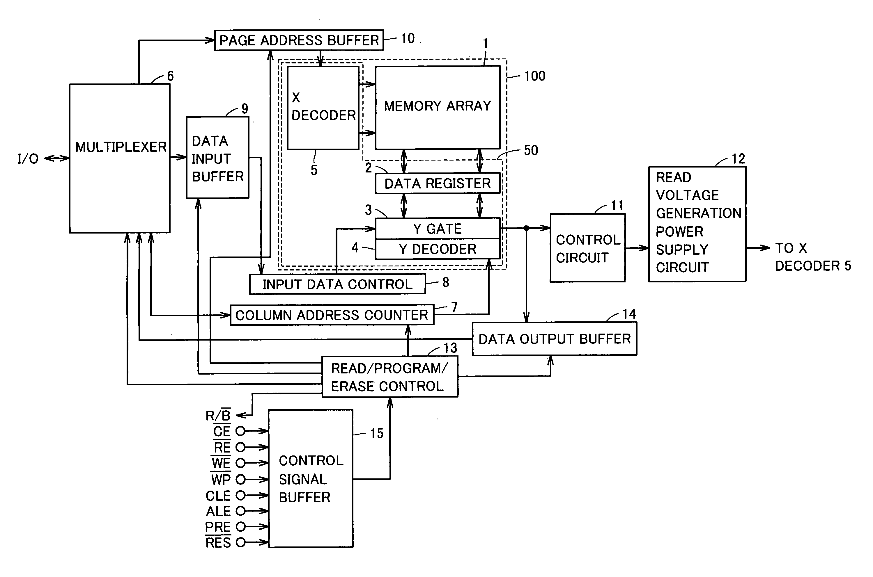
[0032]FIG. 1 is a diagram showing a structure of a semiconductor storage device according to a first embodiment of the present invention.

[0033] With reference to FIG. 1, the semiconductor storage device includes a bank 100, multiplexer 6, a column address counter 7, an input data control 8, a data input buffer 9, a page address buffer 10, a control circuit 11, a read voltage generation power supply circuit 12, a read.program.erase control 13, a data output buffer 14 and a control signal buffer 15.

[0034] Bank 100 includes a memory array 1, a data register 2, a Y gate 3, a Y decoder 4 and an X decoder 5. The semiconductor storage device according to the present embodiment has at least one bank 100.

[0035] Memory array 1 includes a plurality of memory cells for ordinary use. Memory array 1 also includes at least one RMC (Reference Memory Cell) having the same structure as that of a memory cell for ordinary use.

[0036] Data register 2, Y gate 3, Y decod...

second embodiment

[0099] The present embodiment relates to a semiconductor storage device which prevents a reading error due to Vth fluctuation which is caused by the effect of memory cells in adjacent word lines on the opposite sides. Structure and basic operation of the semiconductor storage device according to the present embodiment are the same as those of the semiconductor storage device according to the first embodiment.

[Operation]

[0100]FIG. 13 is a flow chart which defines a procedure of operation executed when the semiconductor storage device according to the second embodiment of the present invention reads data. In the following, description will be made assuming that word lines WL-A, WL-B and WL-C are adjacent and a memory cell to be read is connected to word line WL-B.

[0101] First, the semiconductor storage device externally receives input of an address signal and a command signal indicative of data reading (Steps S11 to S13).

[0102] Next, prior to data reading from a memory cell to be ...

third embodiment

[0113] The present embodiment relates to a semiconductor storage device which prevents a reading error due to Vth fluctuation which is caused by the effect of memory cells in adjacent word lines on the opposite sides and in the same word line.

[0114]FIG. 16 is a schematic diagram showing a structure of memory array 1 in the semiconductor storage device according to the third embodiment of the present invention.

[0115] With reference to FIG. 16, memory array 1 includes word lines WL-A, WL-B and WL-C. Word lines WL-A, WL-B and WL-C are adjacent. In each word line, memory cells and RMCs corresponding to pages 0 to 3 are disposed. In the following, description will be made assuming that a memory cell to be read is a memory cell corresponding to page 0 in word line WL-B. The remaining part of the structure and basic operation are the same as those of the semiconductor storage device according to the first embodiment.

[Operation]

[0116]FIG. 17 is a flow chart which defines a procedure of ...


PUM


Abstract

A semiconductor storage device which includes a memory array including a plurality of memory cells for storing data by using a difference in a threshold voltage and at least one reference cell for storing data indicative of a state of a corresponding memory cell by using a difference in a threshold voltage, a control circuit for determining a read voltage based on data stored by a reference cell corresponding to a memory cell adjacent to a memory cell to be read, a read unit for executing reading from a memory cell to be read by using a determined read voltage, and a write unit for executing writing, when executing writing to a memory cell to be written to bring the memory cell into a written state, data indicating that the memory cell is in the written state to a reference cell corresponding to the memory cell.

Description

BACKGROUND OF THE INVENTION [0001] 1. Field of the Invention [0002] The present invention relates to a semiconductor storage device and, more particularly, a semiconductor storage device having a memory cell for storing data by using a difference in a threshold voltage. [0003] 2. Description of the Background Art [0004] A semiconductor storage device capable of storing information by injecting electrons into a floating gate (FG) or extracting the electrons has been developed such as a flash memory. Flash memory includes a memory cell having a floating gate, a control gate, a source and a drain. Memory cell has its threshold voltage increased when electrons are injected into the floating gate and has its threshold voltage decreased when the electrons are extracted from the floating gate. [0005] Here, scale-down of a semiconductor process makes an expansion of a distribution of Vth (threshold voltage) derived from FG-FG coupling (hereinafter referred to as Vth fluctuation) be extremel...

Claims


Application Information

Patent Timeline
Patent Type & Authority Applications(United States)
IPC IPC(8): G11C11/34
CPCG11C16/3418G11C17/00
Inventor OKAYAMA, SHOTAMATSUBARA, KEN
Owner RENESAS ELECTRONICS CORP
Why Eureka
Try Eureka