Semiconductor device having guard ring and manufacturing method thereof

a technology of shielding ring and shielding plate, which is applied in the direction of semiconductor/solid-state device details, digital storage, instruments, etc., can solve problems such as connection failure in deformed contact holes, and achieve the effect of preventing contact hole deformation

Inactive Publication Date: 2007-01-18
FUJITSU SEMICON LTD
View PDF7 Cites 12 Cited by
  • Summary
  • Abstract
  • Description
  • Claims
  • Application Information

AI Technical Summary

Benefits of technology

[0025] The present invention is made in light of the above problem. It is an object of the present invention to provide a semiconductor device and a manufacturing method thereof which enable the prevention of deformation of contact holes formed in an interlayer insulation film to realize stable contact.
[0026] As a result of assiduous studies, the inventor of the present application has found out that, in the prior manufacturing method, since the guard ring trench divides the interlayer insulation film over a wide range and high-temperature annealing is carried out in this state, the interlayer insulation film greatly suffers heat shrinkage to cause contact hole deformation. Such a phenomenon similarly occurs when the plural guard rings are provided. The inventor of this application has also found out that, in the prior manufacturing method, the contact hole deformation is caused in the case of forming the plural guard rings since the length thereof is not taken into consideration. As a result of the assiduous studies of the inventor of this application, the deformation amount of a contact hole is the largest at a division part (guard ring), and gradually decreases as the distance from this part gets longer. The inventor of this application has also found out that appropriate adjustment of the temperature of heat treatment alleviates the heat shrinkage of the interlayer insulation film so that the contact hole deformation can be alleviated. This means that the deformation amount of a contact hole also depends on the process temperature after it is formed.
[0029] A second manufacturing method of a semiconductor device according to the present invention aims at a manufacturing method of a semiconductor device including a semiconductor substrate, an integrated circuit part formed on the semiconductor substrate, and a guard ring part formed on the semiconductor substrate and surrounding the integrated circuit part to prevent moisture intrusion from the outside. According to this manufacturing method, an interlayer insulation film is first formed on or above the semiconductor substrate to extend over the integrated circuit part and the guard ring part, and contact holes are formed in the interlayer insulation film in the integrated circuit part. Next, a wiring layer is buried in each of the contact holes, and a trench is subsequently formed in the interlayer insulation film in the guard ring part. Thereafter, a buried conductive layer is buried in the trench.
[0031] A third manufacturing method of a semiconductor device according to the present invention aims at a manufacturing method of a semiconductor device including a semiconductor substrate, an integrated circuit part formed on the semiconductor substrate, and a guard ring part formed on the semiconductor substrate and surrounding the integrated circuit part to prevent moisture intrusion from the outside. According to this manufacturing method, first in the integrated circuit part, a gate insulation film and a gate electrode are formed on the semiconductor substrate, and a pair of impurity diffusion layers are formed in a surface of the semiconductor substrate to sandwich the gate electrode in a plan view. Next, a first interlayer insulation film covering at least the gate electrode and the pair of impurity diffusion layers is formed to extend over the integrated circuit part and the guard ring part, and contact holes reaching at least the pair of impurity diffusion layers and a plurality of first trenches reaching the semiconductor substrate in the guard ring part are formed in the first interlayer insulation film. Thereafter, a wiring layer connected to at least the pair of impurity diffusion layers via the contact holes is formed on the first interlayer insulation film, and a first buried conductive layer is buried in each of the first trenches. Note that, according to this manufacturing method, in the step of forming the plural first trenches, the plural first trenches are formed discontinuously, and each of the plural first trenches is formed to be shorter as the distance thereof to a contact hole among the contact holes which is positioned nearest to the first trench itself is shorter.
[0032] According to this third manufacturing method, appropriate adjustment of the length of each of the trenches formed in the guard ring part enables the prevention of contact hole deformation.
[0034] According to this fourth manufacturing method, appropriate adjustment of the temperature of heat treatment while the contact holes are in an opened state enables the prevention of contact hole deformation.

Problems solved by technology

The occurrence of such contact hole deformation is liable to cause connection failure in the deformed contact holes.

Method used


Image

  • Semiconductor device having guard ring and manufacturing method thereof
  • Semiconductor device having guard ring and manufacturing method thereof
  • Semiconductor device having guard ring and manufacturing method thereof

Examples


first embodiment

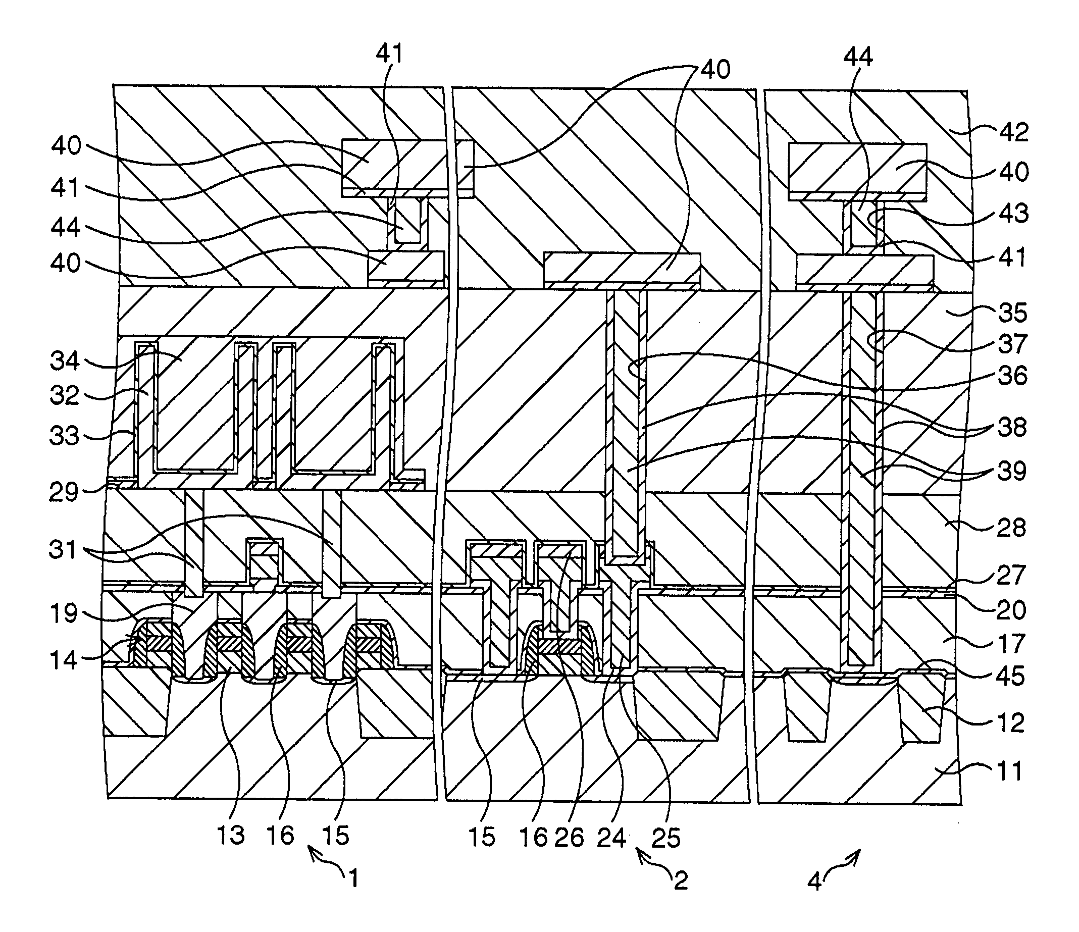
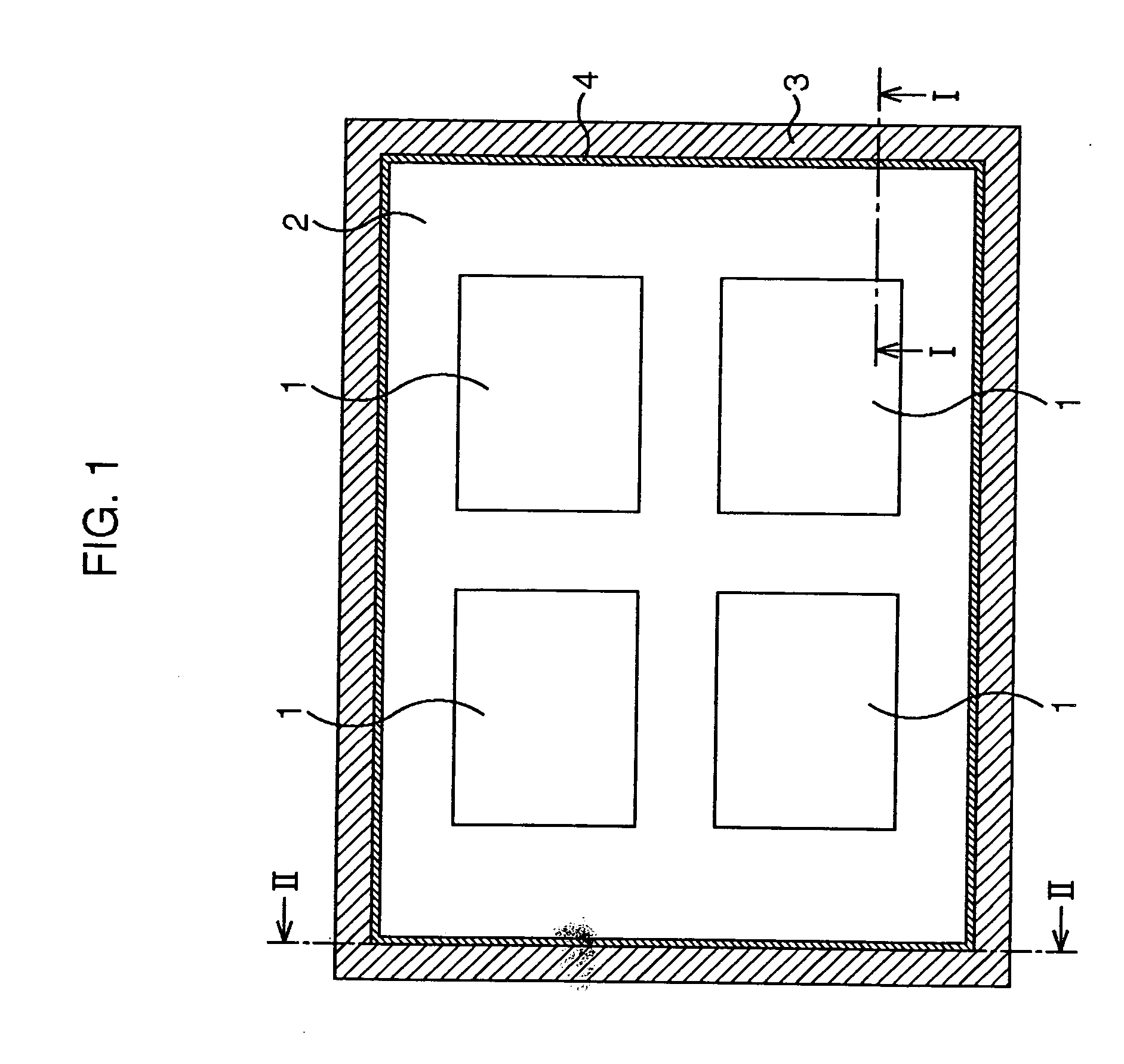
[0068] The first embodiment of the present invention will be first explained. A DRAM (semiconductor device) according to this embodiment is roughly defined into a memory cell array part 1 having a memory cell array provided therein, a peripheral circuit part 2 having drive circuits of memory cells and so on, and a dicing line part 3 on an outer periphery of a chip. Between the peripheral circuit part 2 and the dicing line part 3, a guard ring part (moisture resistant ring part) 4 is provided. The memory cell array part 1 and the peripheral circuit part 2 constitute an integrated circuit part.

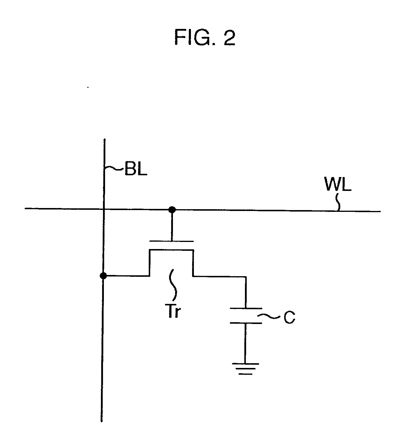
[0069]FIG. 2 is a circuit diagram showing the structure of a memory cell provided in the array part 1. Each memory cell has a capacitor C and a MOS transistor Tr. A gate of the MOS transistor Tr is connected to a word line WL. A source / drain thereof is connected to a bit line BL while the other source / drain is connected to a storage electrode of the capacitor C. An opposing electrode of the cap...

second embodiment

[0095] Next, the second embodiment of the present invention will be explained. FIG. 13 is a schematic plan view showing the structure of a semiconductor device according to the second embodiment of the present invention.

[0096] In the second embodiment, unlike the first embodiment, contact holes 22 and 23 are formed in a peripheral circuit part 2 and at the same time, trenches 47 reaching a diffusion layer 15 are formed in a guard ring part 4. Note that the trenches 47 are arranged discontinuously in the guard ring part 4 provided on the boundary between the peripheral circuit part 2 and a dicing line part 3 as shown in FIG. 13, and each of the trenches 47 has a length so as to satisfy the correlation shown in FIG. 11. In other words, the length of each of the trenches 47 is determined according to the distance to the contact hole 22 or 23 in the peripheral circuit part 2 that is formed at the nearest position to this trench 47. More specifically, the shorter the distance to the con...

third embodiment

[0099] Next, the third embodiment of the present invention will be explained. In the third embodiment, similarly to the first embodiment, a guard ring is formed in a ring shape. But it is different from the first embodiment in a layer structure thereof. FIG. 14 is a schematic plan view showing the structure of a part of a guard ring part of a semiconductor device according to the third embodiment of the present invention. FIG. 15 to FIG. 17 are sectional views taken along III-III line, IV-IV line, and V-V line in FIG. 14, respectively.

[0100] In this embodiment, similarly to the second embodiment, contact holes 22 and 23 are formed, and at the same time, trenches 47 are formed in an interlayer insulation film 17 in a guard ring part 4, being discontinuously arranged. At this time, the length of each of the trenches 47 is adjusted based on the same rule as in the second embodiment so as to satisfy the correlation shown in FIG. 11.

[0101] Thereafter, in each of the trenches 47, a barr...


PUM


Abstract

An interlayer insulation film is etched to form contact holes in an integrated circuit part. At this time, a trench is not formed in a guard ring part. Subsequently, ion implantation is carried out in source / drain regions in a peripheral circuit part for contact compensation, and high-temperature annealing is carried out in order to activate implanted impurities. Subsequently, an interlayer insulation film, a storage capacitor, and another interlayer insulation film are formed in sequence. Then, contact holes reaching a part of wiring layers are formed in the peripheral circuit part while, in the guard ring part, a trench reaching a diffusion layer is formed. Next, a barrier metal film is formed in each of the contact holes and the trench, and further, a contact plug comprising, for example, a W film is buried therein.

Description

CROSS-REFERENCE TO RELATED APPLICATIONS [0001] This application is a divisional of U.S. patent application Ser. No. 10 / 650,810 filed on Aug. 29, 2003, which is based upon and claims priority of Japanese Patent Application No. 2002-255332, filed on Aug. 30, 2002, the contents of which is incorporated by reference in its entirety. Priority under 35 U.S.C. ″120 and 121 is also hereby claimed for benefit of the filing date of U.S. patent application Ser. No. 10 / 650,810.BACKGROUND OF THE INVENTION [0002] 1. Field of the Invention [0003] The present invention relates to a semiconductor device suitable for very large scale integration and a manufacturing method thereof. [0004] 2. Description of the Related Art [0005] A DRAM (Dynamic Random Access Memory) is roughly defined into a memory cell array part having a memory cell array provided therein, a peripheral circuit part having drive circuits of memory cells and so on, and a dicing line part on an outer periphery of a chip. Between the pe...

Claims


Application Information

Patent Timeline
Patent Type & Authority Applications(United States)
IPC IPC(8): H01L29/76G11C7/00H01L23/52H01L21/3205H01L21/82H01L21/822H01L21/8242H01L23/00H01L23/485H01L27/04H01L27/108
CPCH01L23/485H01L23/564H01L27/10885H01L27/10894H01L2924/0002H01L2924/13091H01L2924/00H10B12/482H10B12/09
Inventor YOSHIZAWA, KAZUTAKASATO, KAZUKIIKEMASU, SHINICHIROH
Owner FUJITSU SEMICON LTD
Why Eureka
Try Eureka