

Manufacturing method of P type group III nitride semiconductor layer and light emitting device
a technology of nitride semiconductor layer and manufacturing method, which is applied in the direction of semiconductor devices, basic electric elements, electrical apparatus, etc., can solve the problems of low activation rate of impurities, failure to obtain a low-resistance p type gallium nitride semiconductor layer, nitrogen escape from the group iii nitride semiconductor layer, etc., and achieve high-performance light-emitting
- Summary
- Abstract
- Description
- Claims
- Application Information
AI Technical Summary
Benefits of technology
Problems solved by technology
Method used
Image

Examples
example 1
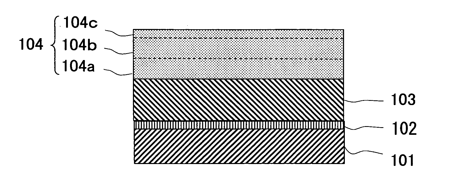
[0038] In order to confirm the activation of the p type impurities in the manufacturing method of the present invention, a GaN buffer layer 102, an undoped GaN layer 103, a p type GaN layer 105 were grown on a substrate 101 made of sapphire as shown in FIG. 3. Specifically, the substrate 101 made of sapphire was set at a predetermined position within a growth furnace for MOCVD as a film forming apparatus, so that a (0001)-oriented plane of sapphire was a growth plane. Then, the GaN buffer layer 102 was grown at 600° C. That is, the GaN buffer layer 102 was grown in a thickness of 20 nm by using trimethyl gallium (TMG:Ga(CH3)3) and ammonia (NH3) gas as material gas.
[0039] Subsequently, the temperature of the substrate 101 was raised to 1050° C., and at this growth temperature, the undoped GaN layer 103 was grown as the under layer of the p type GaN layer 105. The undoped GaN layer 103 was grown in a thickness of 2 μm by using TMG and ammonia gas as material gas.
[0040] Thereafter, a...
example 2
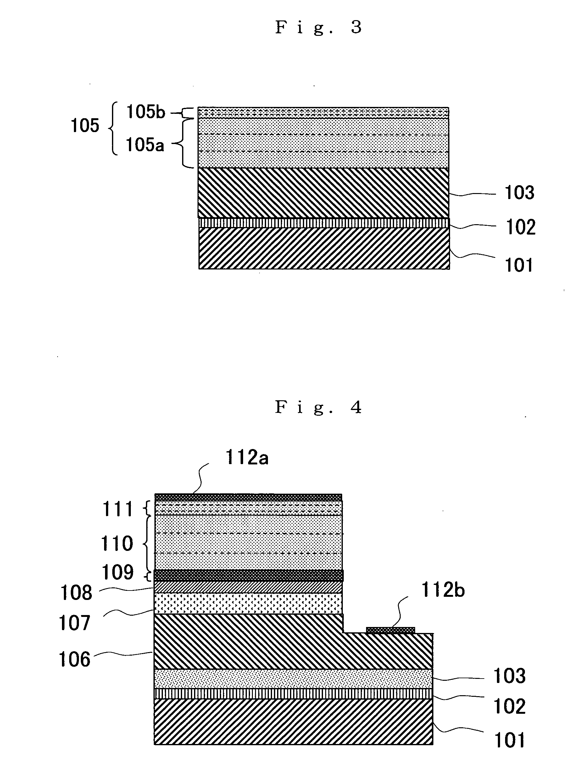
[0045] A light emitting device (LED) as shown in FIG. 4 was manufactured with the manufacturing method of the p type group III nitride semiconductor layer 104 in the present invention.
[0046] A substrate 101 made of sapphire was set at a predetermined position within a growth furnace for MOCVD so that its (0001)-oriented plane was a growth plane. Then, the GaN buffer layer 102 was grown at 600° C. Specifically, the GaN buffer layer 102 was grown in a thickness of 20 nm by using TMG and ammonia gas as material gas.
[0047] Subsequently, the temperature of the substrate 101 was raised to 1050° C., and at this growth temperature, an undoped GaN layer 103 was grown as the under layer of an n type GaN layer 106. The undoped GaN layer 103 was grown in a thickness of 2 μm by using TMG and ammonia gas as material gas.
[0048] After raising the temperature of the substrate 101 to 1050° C., an Si-doped n type GaN layer 106 was formed in a thickness of 2 μm by using TMG, ammonia gas, and silan (...
PUM
 Abstract
Description
Claims
Application Information