Manufacturing method of wiring board and semiconductor device

a manufacturing method and semiconductor technology, applied in the direction of conductive pattern formation, burglar alarm mechanical actuation, instruments, etc., can solve the problems of low raw material use efficiency, disturbance of the reduction in the manufacturing cost of an antenna, and poor environmental protection, so as to achieve low cost, low cost, and simple process

Inactive Publication Date: 2007-01-25
SEMICON ENERGY LAB CO LTD
View PDF10 Cites 83 Cited by
  • Summary
  • Abstract
  • Description
  • Claims
  • Application Information

AI Technical Summary

Benefits of technology

[0019] By using a manufacturing method of a wiring board according to the invention, a wiring board can be manufactured at low cost by a simple process, without performing complicated steps many times. Furthermore, in the manufacturing method of the invention, a conductive resin pattern and an electroly...

Problems solved by technology

However, in the case where an antenna is formed by patterning a copper foil as described above, copper in a region which is not left as a pattern needs to be treated as waste, and use efficiency of the raw material is low.
Furthermore, copper ...

Method used


Image

  • Manufacturing method of wiring board and semiconductor device
  • Manufacturing method of wiring board and semiconductor device
  • Manufacturing method of wiring board and semiconductor device

Examples


embodiment modes

[0038] Embodiment modes of the invention will be described hereinafter with reference to the drawings. However, the invention is not limited to the following description, and it is easily understood by those skilled in the art that the modes and details can be changed in various ways without departing from the spirit and scope of the invention. Therefore, the invention is not interpreted as being limited to the following description of the Embodiment Modes. In the structure of the invention described hereinafter, reference numerals and symbols denoting the same objects are used in common in different drawings.

embodiment mode 1

(Embodiment Mode 1)

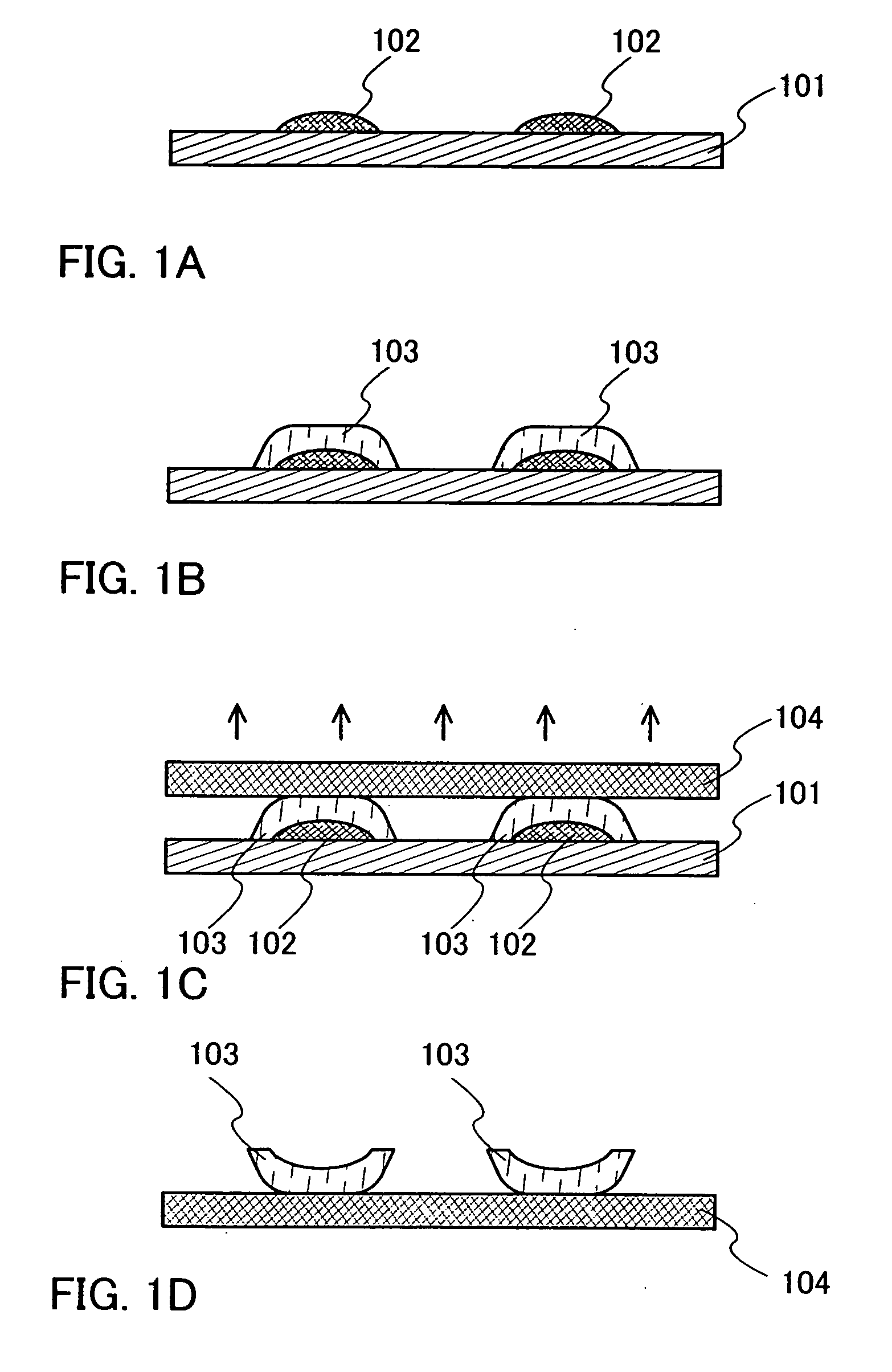
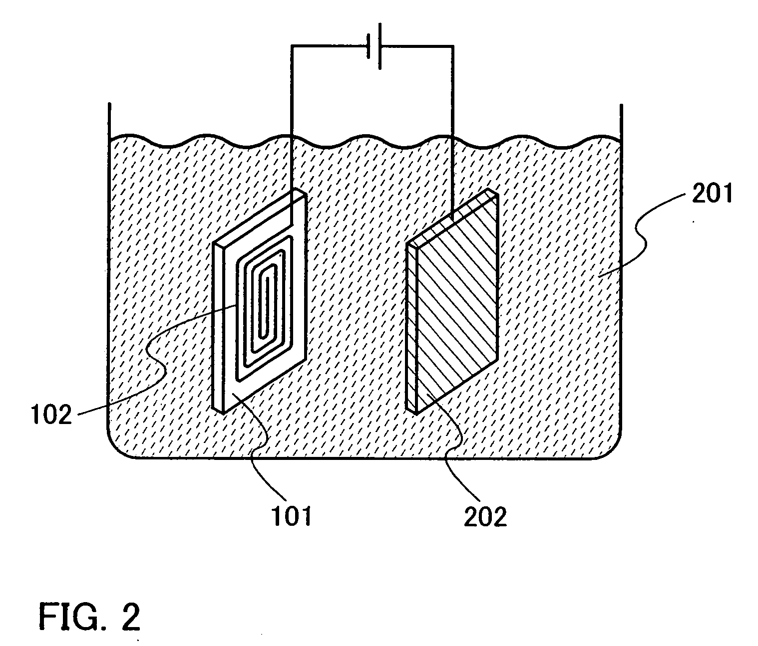
[0039] In this embodiment mode, a formation method of a wiring board by an electrolytic plating process will be described. FIGS. 1A to 1D are cross-sectional views of a manufacturing process of a wiring board of this embodiment mode.

[0040] First, as shown in FIG. 1A, a pattern 102 made of a conductive material is formed over a substrate 101. As the substrate 101, a glass substrate such as barium borosilicate glass or alumino borosilicate glass, a quartz substrate, a ceramic substrate, a silicon substrate or the like can be used. Besides, a substrate made of a flexible synthetic resin such as plastic typified by polyethylene terephthalate (PET), polyethylene naphthalate (PEN), and polyether sulfone (PES), or an acrylic can be used.

[0041] The pattern 102 can be formed by a screen printing method, a vacuum deposition method, a sputtering method, a method in which a conductive material is applied over the entire surface of a glass substrate and then a needless part ...

embodiment mode 2

(Embodiment Mode 2)

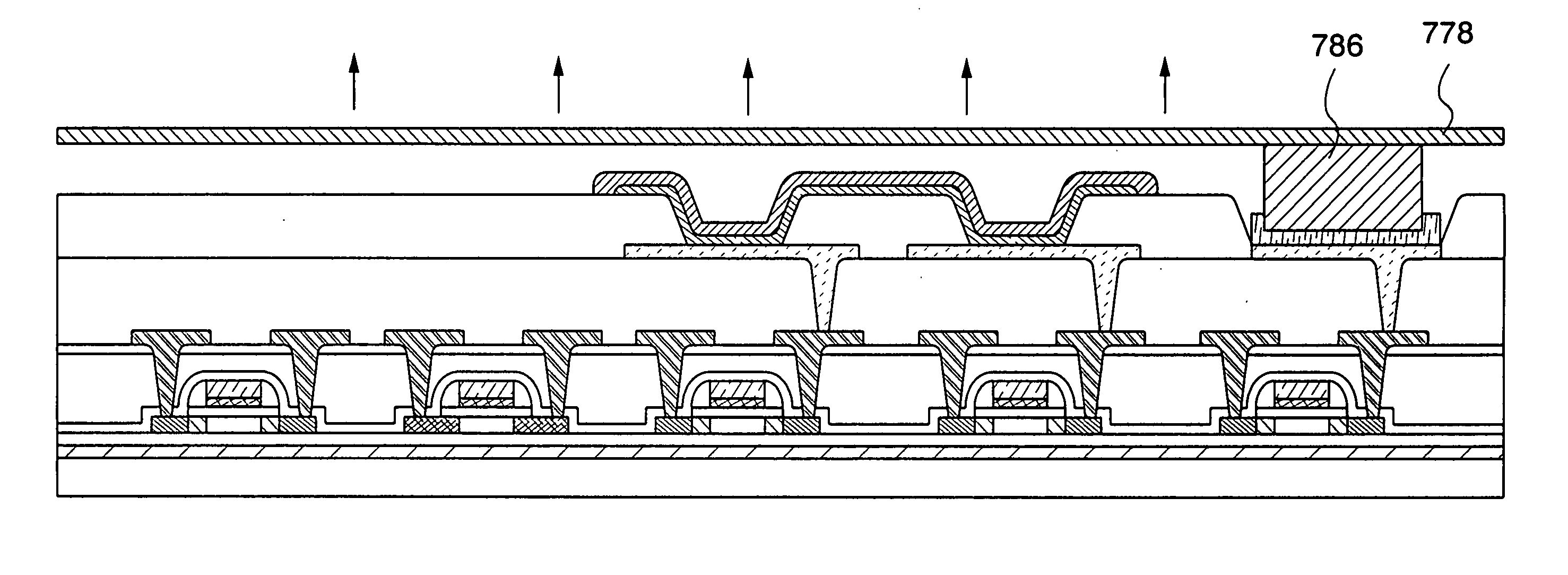
[0047] In this embodiment mode, one mode of a method for connecting a wiring board manufactured according to Embodiment Mode 1 to an IC chip will be described. In this embodiment mode, as shown in FIG. 3A, a semiconductor device in which a conductive film 103 and an IC chip 1140 including a plurality of thin film transistors are provided over a substrate 1141 will be described. It is to be noted that the conductive film 103 is electrically connected to at least one of the thin film transistors included in the IC chip 1140 by connecting the conductive film to the IC chip. In addition, the semiconductor device can exchange data between the IC chip and an external device (reader / writer) without contact, via the conductive film 103. It is to be noted that an element which can communicate data by radio communication is referred to as a semiconductor device in this specification. Such a semiconductor device is also referred to as an IC tag, an ID tag, an RF (Radio Frequ...


PUM

PropertyMeasurementUnit
Electrical conductivityaaaaaaaaaa
Electrical conductoraaaaaaaaaa

Abstract

A manufacturing method of a wiring board and a semiconductor device at low cost and by a simple process, without performing complicated steps many times is proposed. Furthermore, a manufacturing method of a wiring board at low cost and with fewer adverse effects on the environment, and a manufacturing method of a semiconductor device using the wiring board are proposed. A pattern of a conductive material is formed over a first substrate, a conductive film is formed over the pattern by an electrolytic plating process, the pattern and the conductive film are separated, an IC chip including at least one thin film transistor is formed over a second substrate, and the conductive film is electrically connected to the IC chip.

Description

BACKGROUND OF THE INVENTION [0001] 1. Field of the Invention [0002] The present invention relates to a manufacturing method of wiring boards with various shapes and a manufacturing method of a semiconductor device using the wiring board. [0003] 2. Description of the Related Art [0004] In recent years, the necessity of a card equipped with an RFID (Radio Frequency Identification) or a tag equipped with an RFID which can transmit and receive data without contact has been increased in various fields which need automatic identification such as management of valuable securities and merchandise. The card equipped with an RFID reads and writes data from / to an external device without contact, via an antenna with a shape adapted to the frequency band that is used when transmitting and receiving data. The card equipped with an RFID has larger memory capacity and higher security than a magnetic card that records data by a magnetic recording method. Hence, modes of the card equipped with an RFI...

Claims


Application Information

Patent Timeline
IPC IPC(8): H01L21/44
CPCH05K3/205H05K3/245H05K2203/0117H01L2224/11Y10T29/49224Y10T29/49016Y10T29/49144Y10T29/49018Y10T29/49155Y10T29/49117H01L2924/12044H01L2924/00
Inventor MARUYAMA, JUNYAAOKI, TOMOYUKI
Owner SEMICON ENERGY LAB CO LTD
Why Eureka
Try Eureka