
System for molecular imaging
- Summary
- Abstract
- Description
- Claims
- Application Information
AI Technical Summary
Benefits of technology
Problems solved by technology
Method used
Image

Examples
first embodiment
[0084] The detector can be made of different embodiments as shown in FIGS. 5-7. the detector is one pixel detector (FIGS. 5 & 6) or an array of pixel detectors (FIG. 7). FIG. 5 shows fabricated CdZnTe solid state detectors 50. These CdZnTe detectors 50 with pixel electrodes 52 are fabricated and the indium bump 64 bonding is carried out. This process needs high quality solid state detector material such as single or polycrystaline CdZnTe, GaAs, Si, C, Se, Ge, HgI2 and PbI2 material; fabrication of high-quality gold or platinum or other type of electrodes 52 for the pixels 52 and the HV bias pad(s)63. The indium bump bonding is an important technique for producing low-capacitance, high-quality uniform bonds between detector arrays and ASICs (Application Specific Integrated Circuits). The pixel array consists of 2×2 to 1,000,000×1,000,000 array of 0.001×0.001 to 500×500-micron pitch gold, metal or conductive blocking or non-blocking pixels pads 52 or electrodes (FIG. 6).
[0085] A guard...
second embodiment
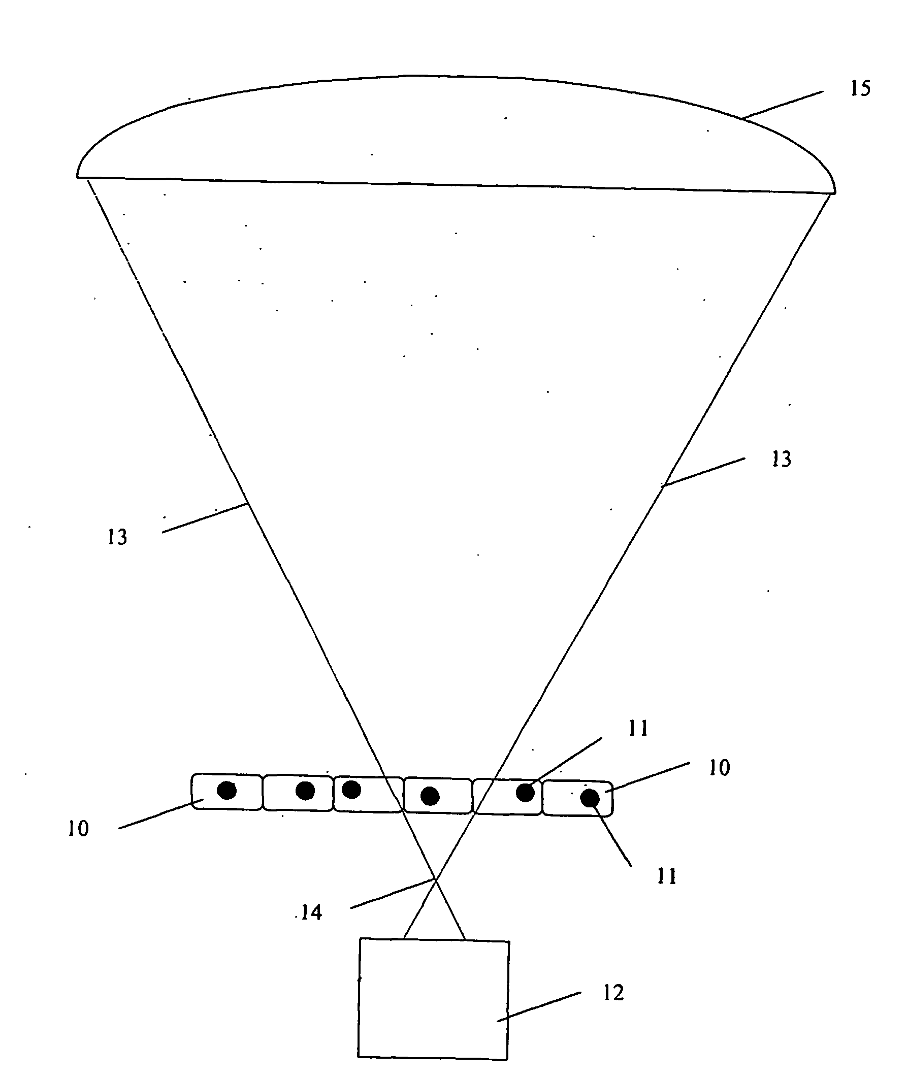
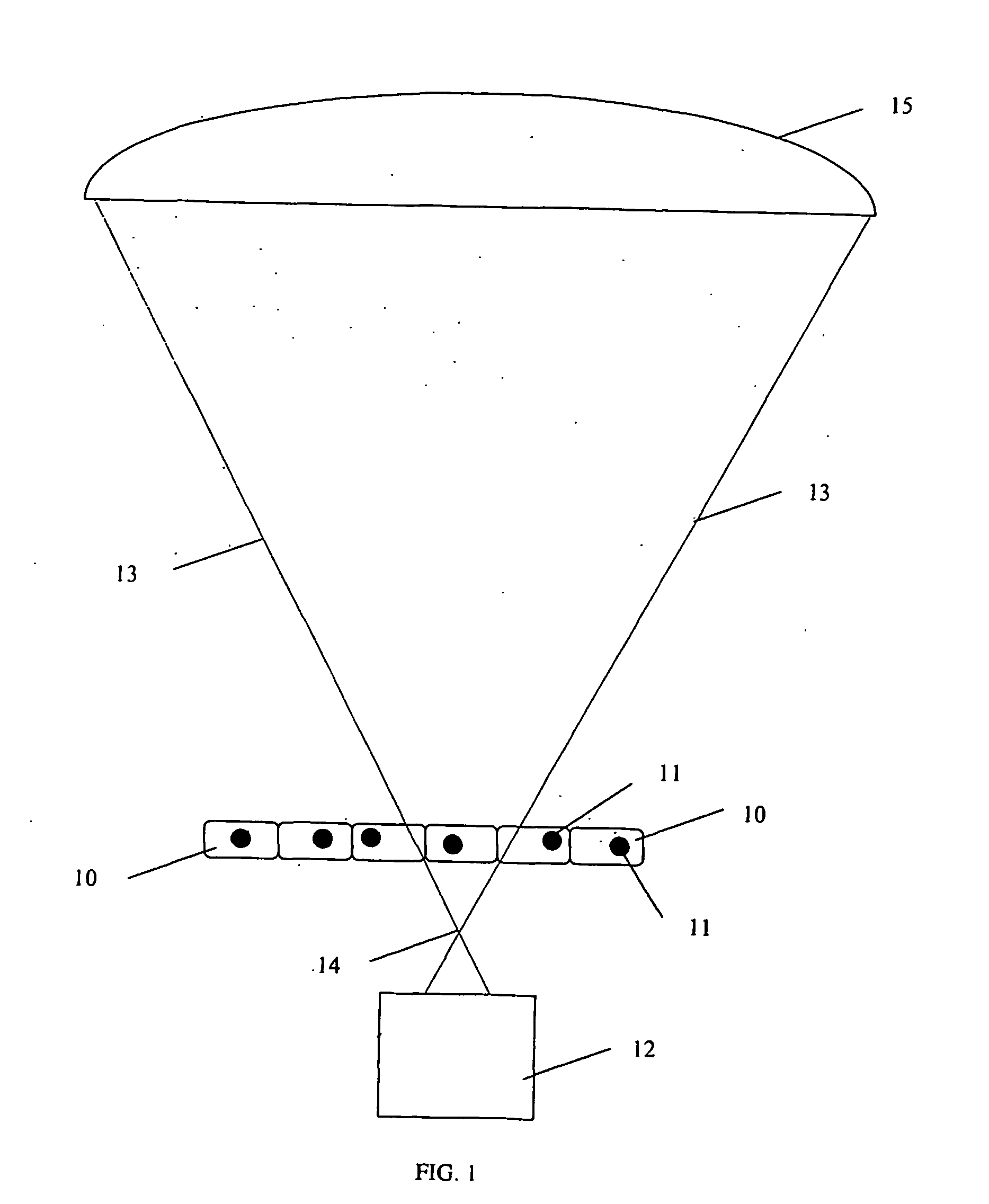
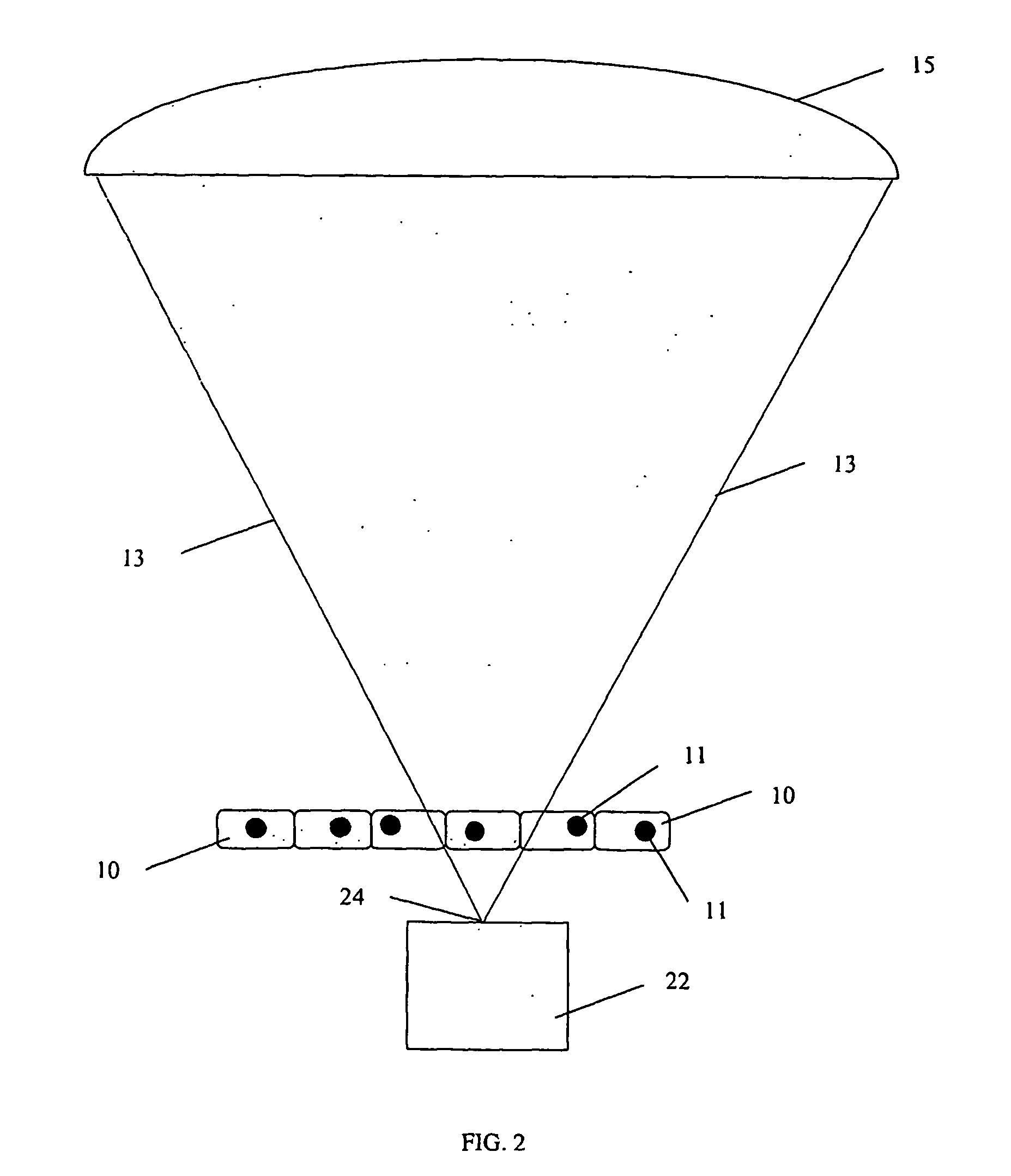
[0090] Molecular imaging instrument imaging cell(s) 10 with possible nuclei 11. Generator 22 produces a conic or fan beam 13 of photons 13 and / or particles 13. The beam is generated from a small vertex 24 and diverged from the source point 24. The beam passes through the cell(s) 10 and is imaged by the detector 15. The detector 15 can be formed as discussed above.
[0091] Third emboddiment: Molecular imaging instrument imaging cell(s) 10 using a parallel beam 34 of photons 34 or particles 34 originated from a generator 32 then goes through the cell(s) 10. A device 35 diverges the beams to magnify and image cell(s) on the detector 15. The detector 15 can be formed as discussed above.
[0092] Fourth emboddiment: Molecular imaging instrument imaging cell(s) using a photons 43 or particles 43 emitted from the radiochemicals or radiopharmaceutical inside the cell. A device 45 magnifies and / or focusses the photons or particles onto detector 15 to be imaged. The detector 15 can be formed as ...
PUM
 Abstract
Description
Claims
Application Information