

Low voltage organic electroluminescent element
a low-voltage, organic technology, applied in the direction of discharge tube luminescnet screens, other domestic articles, natural mineral layered products, etc., can solve the problems of device color shift to a less desirable hue, device performance limitations that have represented a barrier to many desirable applications, and bphen/alq mix of seo et al. shows inferior stability, etc., to achieve the effect of maintaining the purity of the color produced and reducing the drive voltage of the oled devi
- Summary
- Abstract
- Description
- Claims
- Application Information
AI Technical Summary
Benefits of technology
Problems solved by technology
Method used
Image

Examples
example 1
Synthesis of A-37
[0212]
[0213] Compound (3), eq. 1, was prepared in the following manner: Under a nitrogen atmosphere, acetylenic compound (2) (2.0 g, 12 mMole), was dissolved in dimethylformamide (DMF) (100 mL) and the solution cooled to 0° C. Potassium t-butoxide (KButO) (1.4 g, 12 mMole), was added and the mixture stirred well for approximately 15 minutes. To this mixture was then added the benzophenone (1) (3.53 g, 30 mMole). Stirring was continued at 0° C. for approximately 30 minutes and then allowed to come to room temperature over a 1-hour period. At the end of this time the solution was cooled to 0° C. and the reaction treated with saturated sodium chloride (20 mL). The mixture was then diluted with ethyl acetate, washed with 2N-HCl (3 times), dried over MgSO4, filtered and concentrated under reduced pressure. The crude product was triturated with petroleum ether to give the product as an off-white solid. The yield of compound (3) was 3.0 g.
[0214] Compound (3) (7.0 g, 15 m...
example 2
Determination of LUMO and HOMO Values
[0215] A comparison of the LUMO values of the first and second compounds in the layer of the invention should be carefully considered. To obtain a drive voltage reduction over devices that contain only a first compound or only a second compound, it is desirable that there is a difference in the LUMO values of the compounds. The first compound should have a lower LUMO (more negative) value than the second compound, or compounds.
[0216] Additionally, a comparison of the HOMO values of the hole-blocking material and the material in the light-emitting layer should be considered carefully. To obtain effective hole blocking it is desirable that there is a difference between the HOMO values of the LEL and HBL materials.
[0217] The LUMO and HOMO values are typically determined experimentally by electrochemical methods. A Model CHI660 electrochemical analyzer (CH Instruments, Inc., Austin, Tex.) was employed to carry out the electrochemical measurements....
example 3
Determination of Low-Voltage Electron Transport Materials
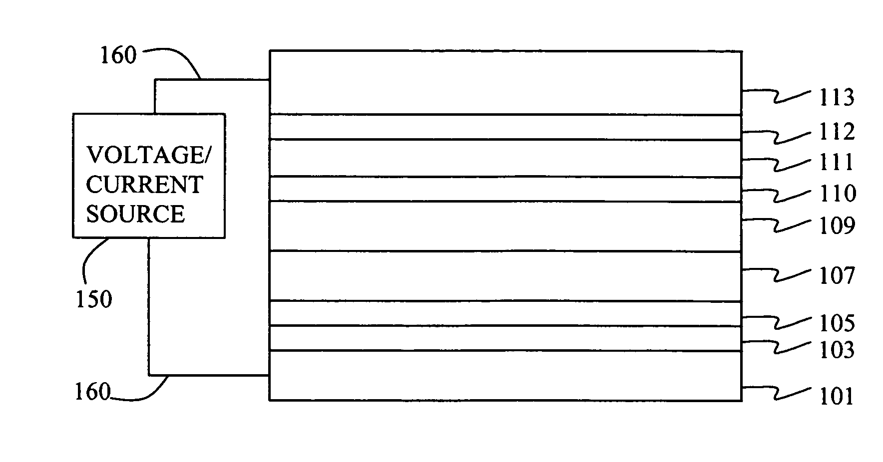
[0223] Materials were tested to determine if they were low voltage electron transport materials by incorporating them alone into the electron-transporting layer of a device. Devices were constructed in the following manner.
[0224] A glass substrate coated with an 21.5 nm layer of indium-tin oxide (ITO) as the anode was sequentially ultrasonicated in a commercial detergent, rinsed in deionized water, degreased in toluene vapor and exposed to oxygen plasma for about 1 min. [0225] a) Over the ITO was deposited a 1 nm fluorocarbon (CFx) hole-injecting layer (HIL) by plasma-assisted deposition of CHF3. [0226] b) A hole-transporting layer (HTL) of N,N′-di-1-naphthalenyl-N,N′-diphenyl-4,4′-diaminobiphenyl (NPB) having a thickness of 75 nm was then evaporated onto a). [0227] c) A 35 nm light-emitting layer (LEL) of tris(8-quinolinolato)aluminum (III) (Alq) was then deposited onto the hole-transporting layer. [0228] d) A 35 nm electro...
PUM
| Property | Measurement | Unit |
|---|---|---|
| Fraction | aaaaa | aaaaa |
| Time | aaaaa | aaaaa |
| Fraction | aaaaa | aaaaa |
Abstract
Description
Claims
Application Information