Segmented biased peripheral electrode in plasma processing method and apparatus

Inactive Publication Date: 2007-02-08
TOKYO ELECTRON LTD
View PDF20 Cites 51 Cited by
  • Summary
  • Abstract
  • Description
  • Claims
  • Application Information

AI Technical Summary

Benefits of technology

[0011] According to some embodiments of the invention, a multi-segmented ring-shaped electrode is provided for reducing non-uniformities in a semiconductor plasma processing apparatus that is dimensioned to encircle a substrate support. Electrical energy is coupled to each of the segments of the electrode and a controller is programmed to sequentially energize the segments of the electrode.
[0012] The electrode may be included in a semiconductor wafer processing apparatus having a vacuum processing chamber, a sputtering target in the chamber, a high-density plasma source coupled to the chamber, and a substrate support in the chamber with the electrode encircling the substrate support. Electrical energy is coupled to segments of the electrode to sequentially energize the segments of the electrode.
[0013] Azimuthal uniformity of a film applied in an ionized physical vapor deposition (iPVD) process is improved by encircling a substrate support with the segmented element and cyclically energizing the segmented element by sequenti

Problems solved by technology

Of the advantages of ionized PVD systems, there are still some constraints to utilization of the system at the maximum of its performance.
For example, existing hardware does not allow optimizing uniformity for both deposition and etch processes simultaneously over a wide process pressure window.
While an annular target provides excellent conditions for flat field deposition uniformity, the use of large area inductively coupled plasma (ICP) to generate a large size low-pressure plasma for uniform etch process is geometrically

Method used


Image

  • Segmented biased peripheral electrode in plasma processing method and apparatus
  • Segmented biased peripheral electrode in plasma processing method and apparatus
  • Segmented biased peripheral electrode in plasma processing method and apparatus

Examples


Embodiment Construction

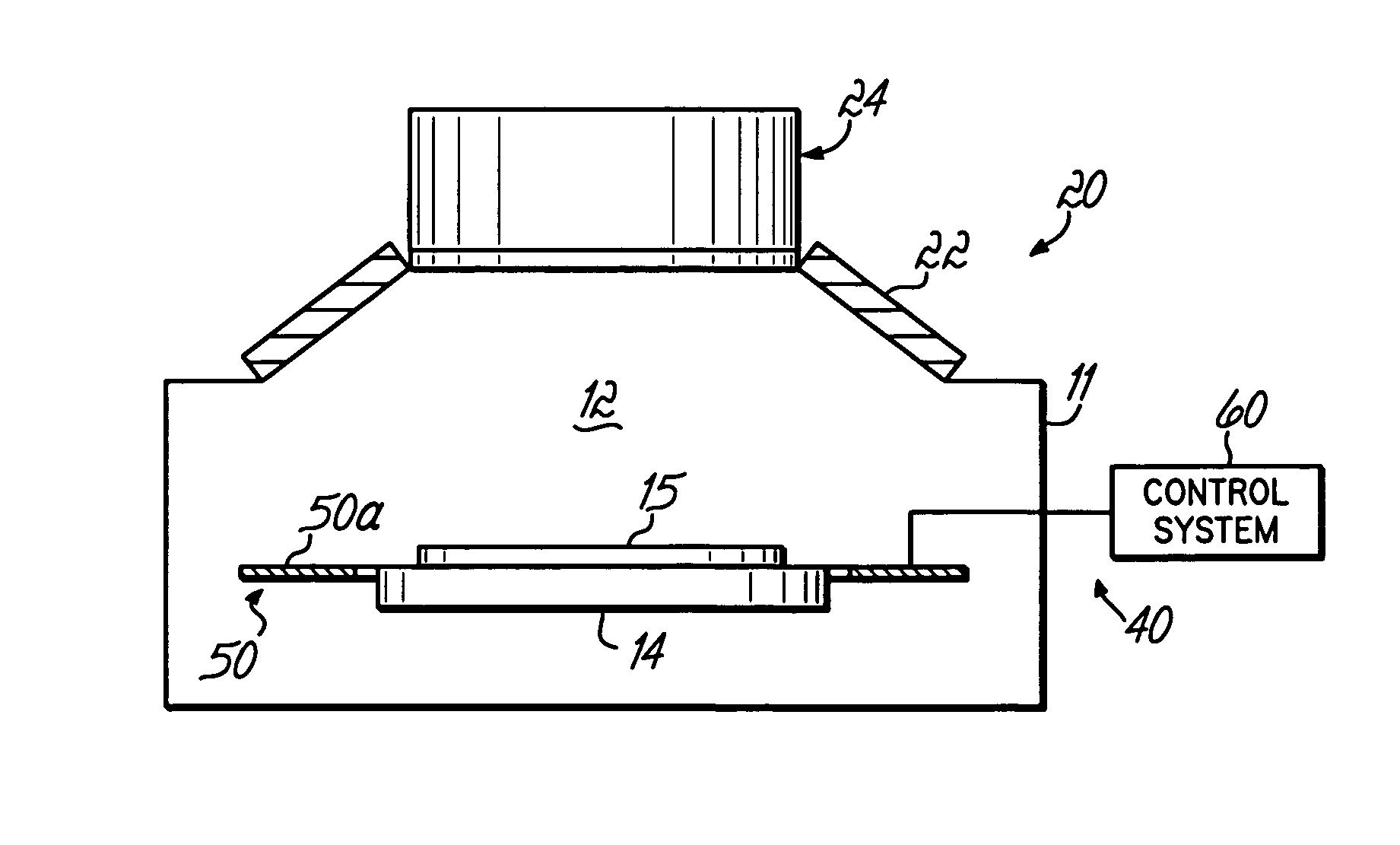
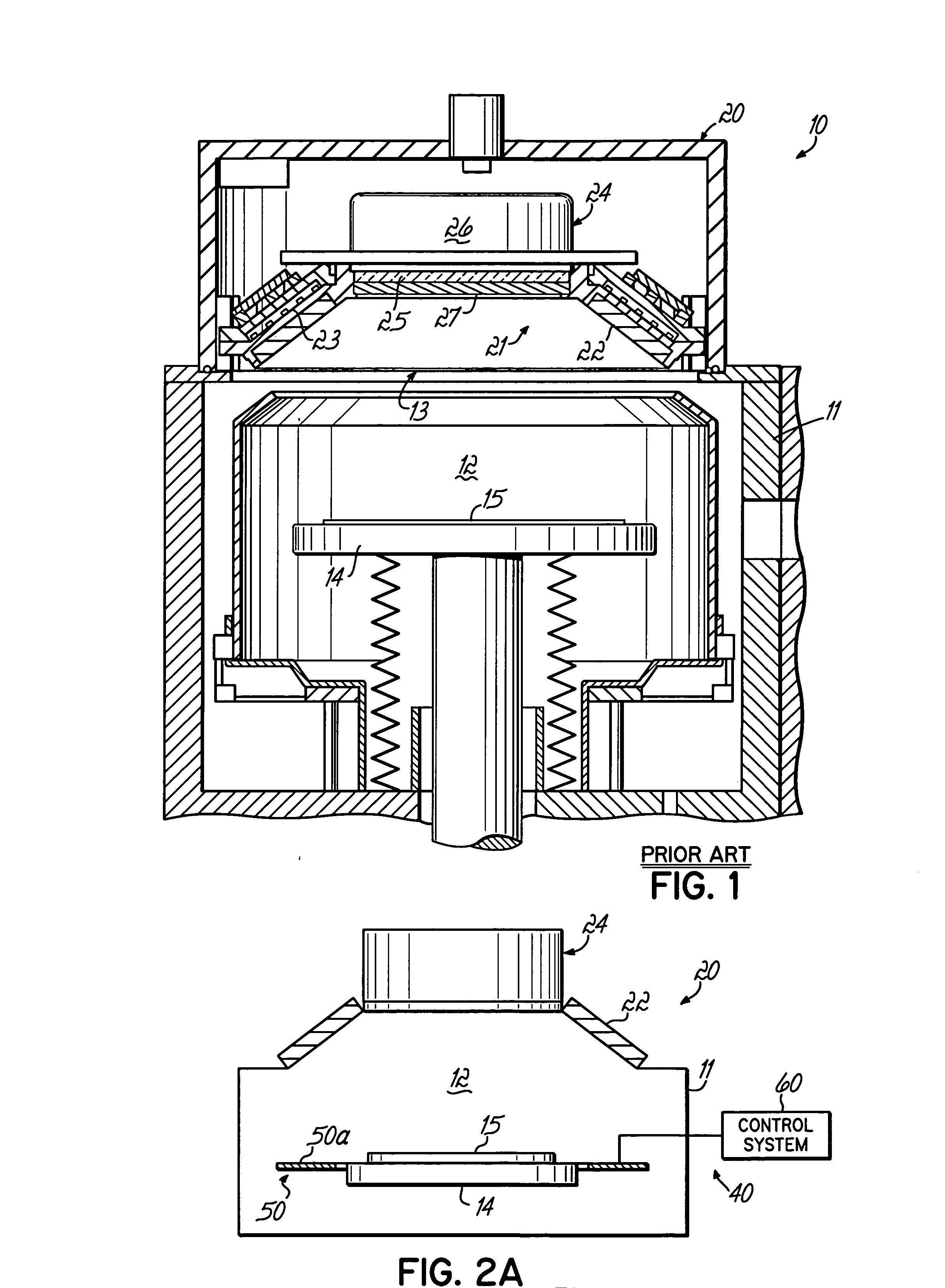
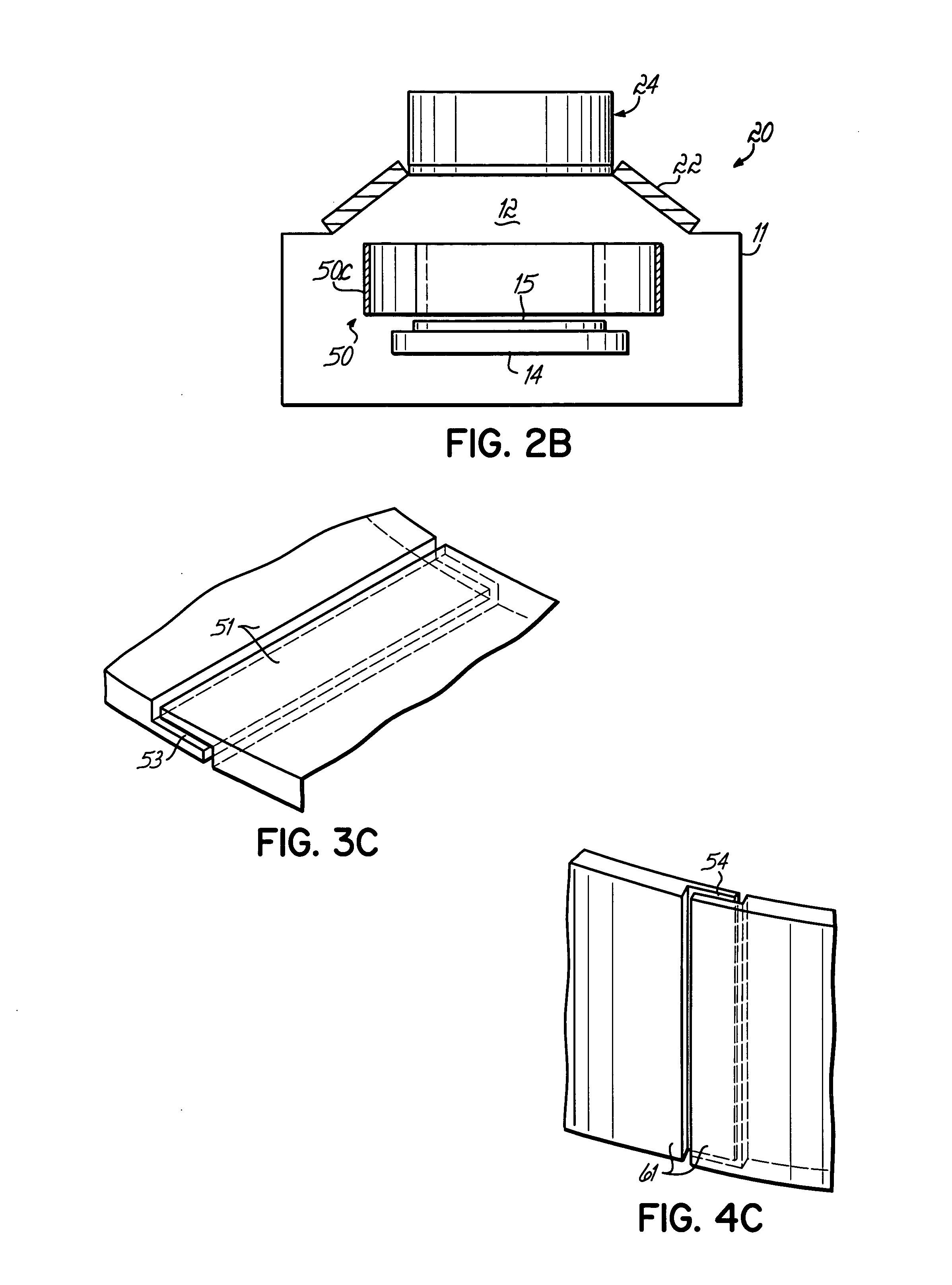
[0028] The concepts of the present invention can be used in various plasma processing systems, such as those for performing sputter etching and deposition processes, plasma-enhanced CVD (PECVD) processes, ionized PVD (iPVD) processes, and reactive ion etching processes (RIE). They are particularly applicable for use in iPVD systems for performing standard and thermalized processes, such as, for example, processes employing an apparatus 10 that is illustrated in FIG. 1. Examples of semiconductor wafer processing machines of the iPVD type are described in U.S. Pat. Nos. 6,080,287, 6,287,435 and 6,719,886, each hereby expressly incorporated by reference herein. Embodiments of the present invention are described in the context of the apparatus 10 of FIG. 1, even though applicable to other types of systems.

[0029] The iPVD apparatus 10, as illustrated, includes a vacuum processing chamber 12 enclosed in a chamber wall 11 having an opening 13 at the top thereof in which is mounted an ioni...


PUM

PropertyMeasurementUnit
Densityaaaaaaaaaa
Distanceaaaaaaaaaa
Circumferenceaaaaaaaaaa

Abstract

A system and method for enhancing the plasma etch process uniformity in an ionized PVD semiconductor wafer processing system is provided. The system and method controls chamber conditions so as to produce highly uniform processing for a deposition-etch process sequence and yielding improved coverage capabilities of high aspect ratio (HAR) features when the deposition and etch steps are performed within same processing chamber. Plasma is generated and maintained by an inductively coupled plasma (ICP) source. In the deposition portions of the process, metal or other coating material is produced from a target of a PVD source. A segmented peripheral electrode surrounds the wafer at a distance from its outer edge. RF induced bias is applied to the electrode, cycling around the segment so as to subject each to a duty cycle controlled by a processor. The tendency of the etching or sputtering of the wafer surface that occurs with deposition to produce a radially selective coverage of the wafer, particularly of inside features and the flat field of the wafer, are offset by the bias electrode. A segmented biased-ring electrode is controlled to provide conditions for azimuthal improvement of etch rate and overall etch rate uniformity across the wafer.

Description

[0001] The present application is related to U.S. patent application Ser. No. 10 / 454,381 (filed Jun. 4, 2003, Pub. US 2005 / 0103444), Ser. No. 10 / 717,268 (filed Nov. 19, 2003, Pub. US 2005 / 0103445) and Ser. No. 10 / 766,505 (filed Jul. 28, 2004), each hereby expressly incorporated by reference herein.FIELD OF THE INVENTION [0002] This invention relates to high-density plasma generating devices, systems and processes, particularly for the manufacture of semiconductor wafers. This invention particularly relates to the high density inductively coupled plasma sources used in semiconductor processing. BACKGROUND OF THE INVENTION [0003] For the deposition of films onto high aspect ratio, submicron-featured semiconductor wafers, an ionized physical vapor deposition (iPVD) process and apparatus are useful. Apparatus having the features as described in U.S. Pat. Nos. 6,287,435, 6,080,287, 6,197,165, 6,132,564 are particularly well suited for the sequential or instant deposition and etching proc...

Claims


Application Information

Patent Timeline
IPC IPC(8): C23C14/00
CPCC23C14/345H01J37/32706H01J37/32623
Inventor BRCKA, JOZEF
Owner TOKYO ELECTRON LTD
Why Eureka
Try Eureka