Structures for reducing operating voltage in a semiconductor device

a technology of operating voltage and semiconductor device, which is applied in the direction of semiconductor lasers, electrical devices, lasers, etc., can solve the problems of device performance degradation, and achieve the effect of reducing the operating voltage of the semiconductor device, and reducing the operating voltag

Inactive Publication Date: 2007-02-15
AVAGO TECH WIRELESS IP SINGAPORE PTE
View PDF7 Cites 34 Cited by
  • Summary
  • Abstract
  • Description
  • Claims
  • Application Information

AI Technical Summary

Benefits of technology

[0005] Structures for reducing operating voltage in a semiconductor device are disclosed. Co-doping one or more tunnel junction material layers with a dopant having an ionization energy higher than the ionization energy of the other dopant reduces the operating voltage of a semiconductor device. Introducing a defect at the interface of two tu

Problems solved by technology

A high series resistance elevates the operating voltage of the device and causes

Method used


Image

  • Structures for reducing operating voltage in a semiconductor device
  • Structures for reducing operating voltage in a semiconductor device
  • Structures for reducing operating voltage in a semiconductor device

Examples


Embodiment Construction

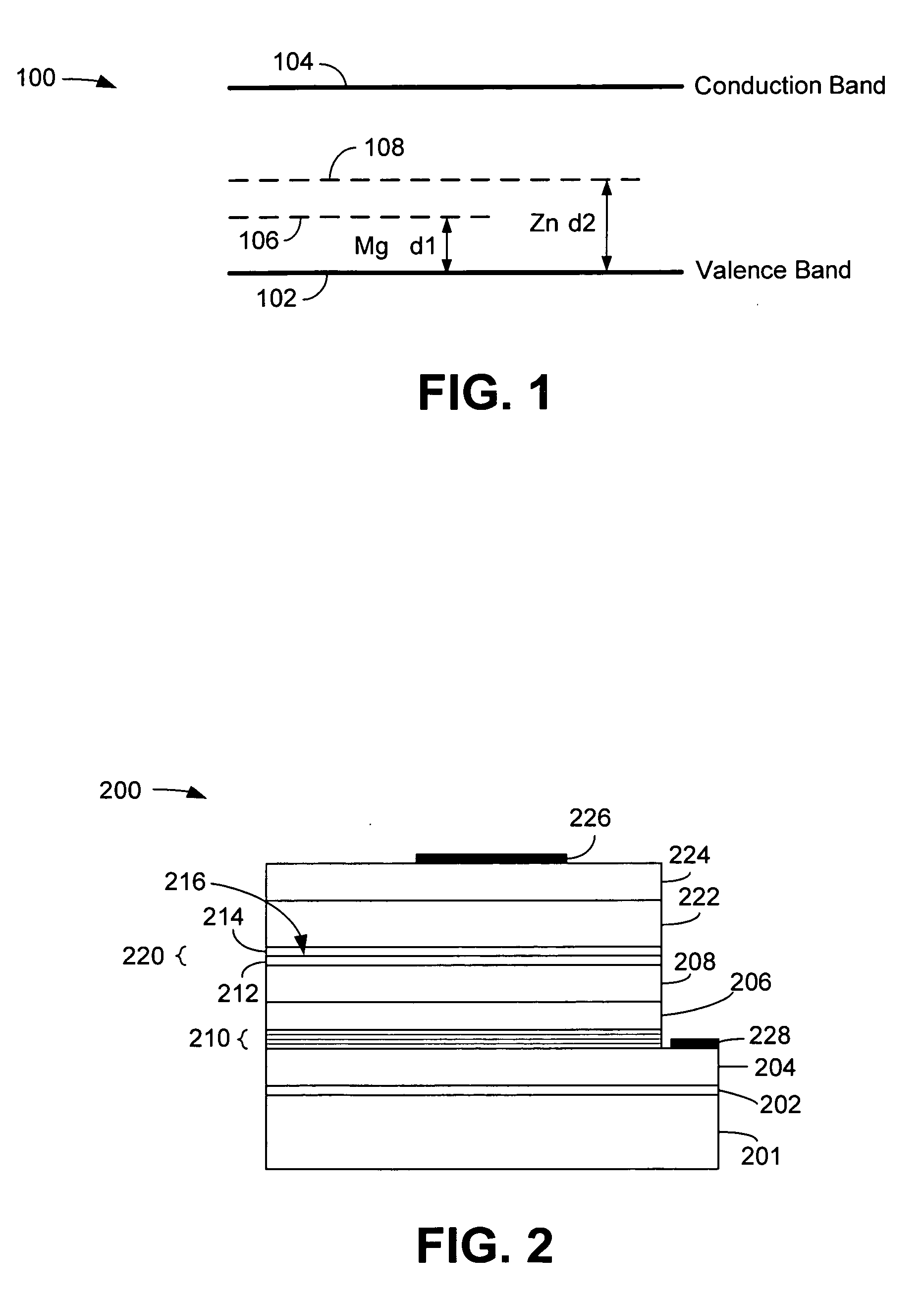
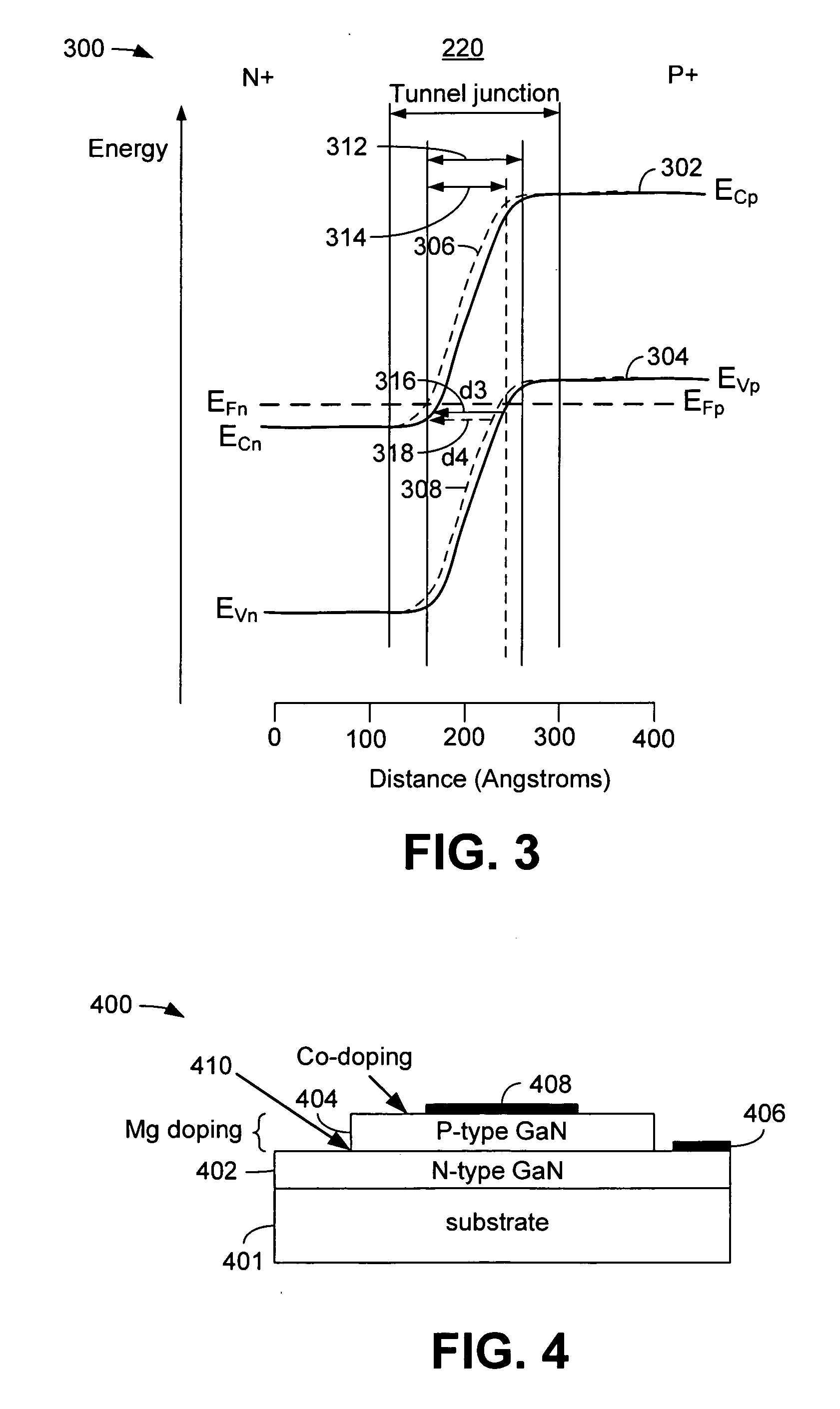
[0019] Embodiments in accordance with the invention are based on the realization that deep acceptor and donor level doping, while having a minimal impact in the bulk semiconductor material, significantly improves the conductivity of the semiconductor material when ionized in the depletion region of a tunnel junction or an ohmic contact. Magnesium is typically used as a p-type dopant and silicon is typically used as an n-type dopant in Group III-V nitride materials. However, additional dopants with a higher ionization energy, or activation, energy (i.e., a “deeper” impurity) will become ionized in the depletion region, appreciably reducing the width of the depletion region, and therefore reducing the operating voltage of a semiconductor device.

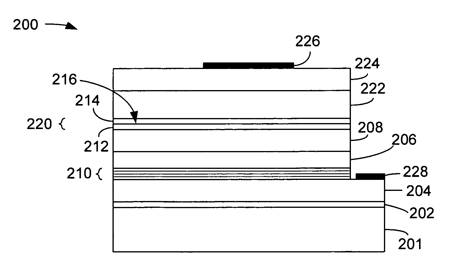
[0020] In an embodiment in accordance with the invention, the voltage drop of a tunnel junction is lowered by forming the tunnel junction structure of a p-type tunnel junction layer and an n-type tunnel junction layer of semiconductor material...


PUM


Abstract

A light-emitting device comprises an active region configured to generate light in response to injected charge, and an n-type material layer and a p-type material layer, wherein at least one of the n-type material layer and the p-type material layer is doped with at least two dopants, at least one of the dopants having an ionization energy higher than the ionization energy level of the other dopant.

Description

BACKGROUND [0001] Semiconductor-based optoelectronic devices are used in optical communication systems and other systems. [0002] Various materials have been used to fabricate optoelectronic light emitting devices. In one example, group III and group V elements are combined in various compositions to form layers. One of the material systems that use group III and group V elements is referred to as the gallium nitride (GaN) material system. Typically, layers of group III-V elements are formed to fabricate a semiconductor optoelectronic device. These devices typically include a region referred to as a p-n junction. One or more p-n junctions may form part of a semiconductor optoelectronic device. [0003] For optoelectronic devices formed using the GaN material system, the contact resistance of the p-type material is typically relatively high compared to the contact resistance of the n-type material. Further, the mobility of holes in the p-type material is typically lower than the mobilit...

Claims


Application Information

Patent Timeline
IPC IPC(8): H01L29/06H01L31/00
CPCH01S5/305
Inventor ROBBINS, VIRGINIA M.LESTER, STEVEN D.MILLER, JEFFREY N.BOUR, DAVID P.
Owner AVAGO TECH WIRELESS IP SINGAPORE PTE
Why Eureka
Try Eureka