DMOSFET and planar type MOSFET

a technology of mosfet and mosfet, which is applied in the direction of semiconductor devices, diodes, electrical apparatus, etc., can solve the problems of insufficient examination of shallow junctions, reduced withstand voltage, and reduced cell miniaturization, so as to reduce diffusion in a lateral direction, low on-resistance, and low feedback capacitance

Inactive Publication Date: 2007-03-01
RENESAS TECH CORP
View PDF13 Cites 49 Cited by
  • Summary
  • Abstract
  • Description
  • Claims
  • Application Information

AI Technical Summary

Benefits of technology

[0014] The feature of the present invention lies in that, in a planar type MOSFET, shallow junction of a channel layer with a channel depth of 0.5 μm or less is formed in order to achieve the low ON-resistance and the low feedback capacitance, and the present invention has features as follows in order to prevent the punch through of a channel layer in which the diffusion in a lateral direction is decreased due to the shallow junction.

Problems solved by technology

However, in the planar type MOSFET of the Patent Document 1, the miniaturization of the cell is insufficient, and the ON-resistance is still high in comparison to the trench MOSFET and the examination for further reduction of the ON-resistance is necessary.
However, in the planar type MOSFET of the Patent Document 1, the depth of the channel layer is about 0.8 Mm, and the examination for the shallow junction is insufficient.
Therefore, the planar type MOSFET has a problem in its structure that the punch through of the channel layer occurs and the withstand voltage is decreased.

Method used


Image

  • DMOSFET and planar type MOSFET
  • DMOSFET and planar type MOSFET
  • DMOSFET and planar type MOSFET

Examples


first embodiment

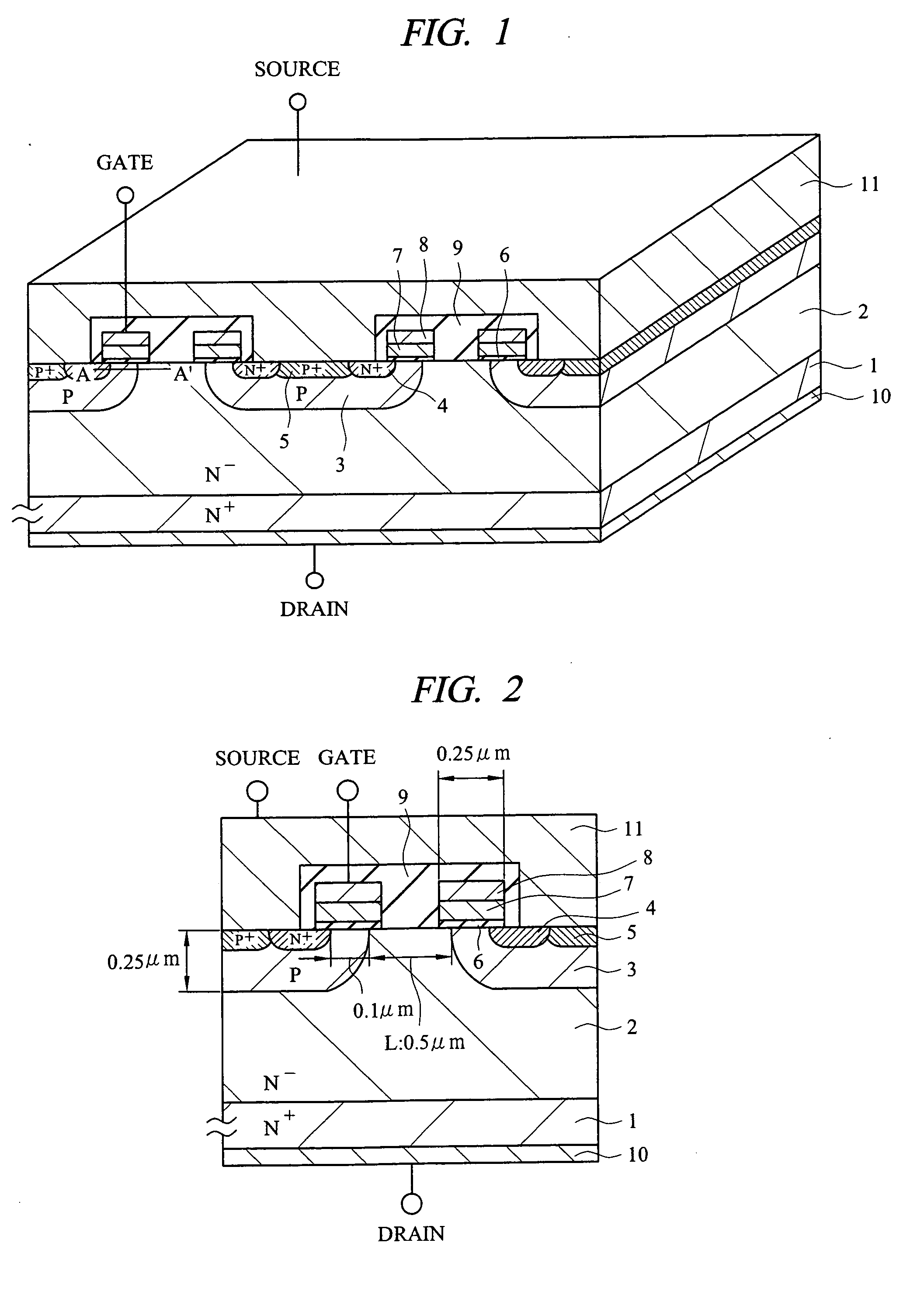
[0059] The first embodiment of the present invention will be described with reference to FIG. 1 to FIG. 8. FIG. 1 is a diagram showing a sectional structure of a planar type MOSFET according to the first embodiment of the present invention. FIG. 2 is a cross-sectional view showing the dimensions of the planar type MOSFET according to the first embodiment of the present invention.

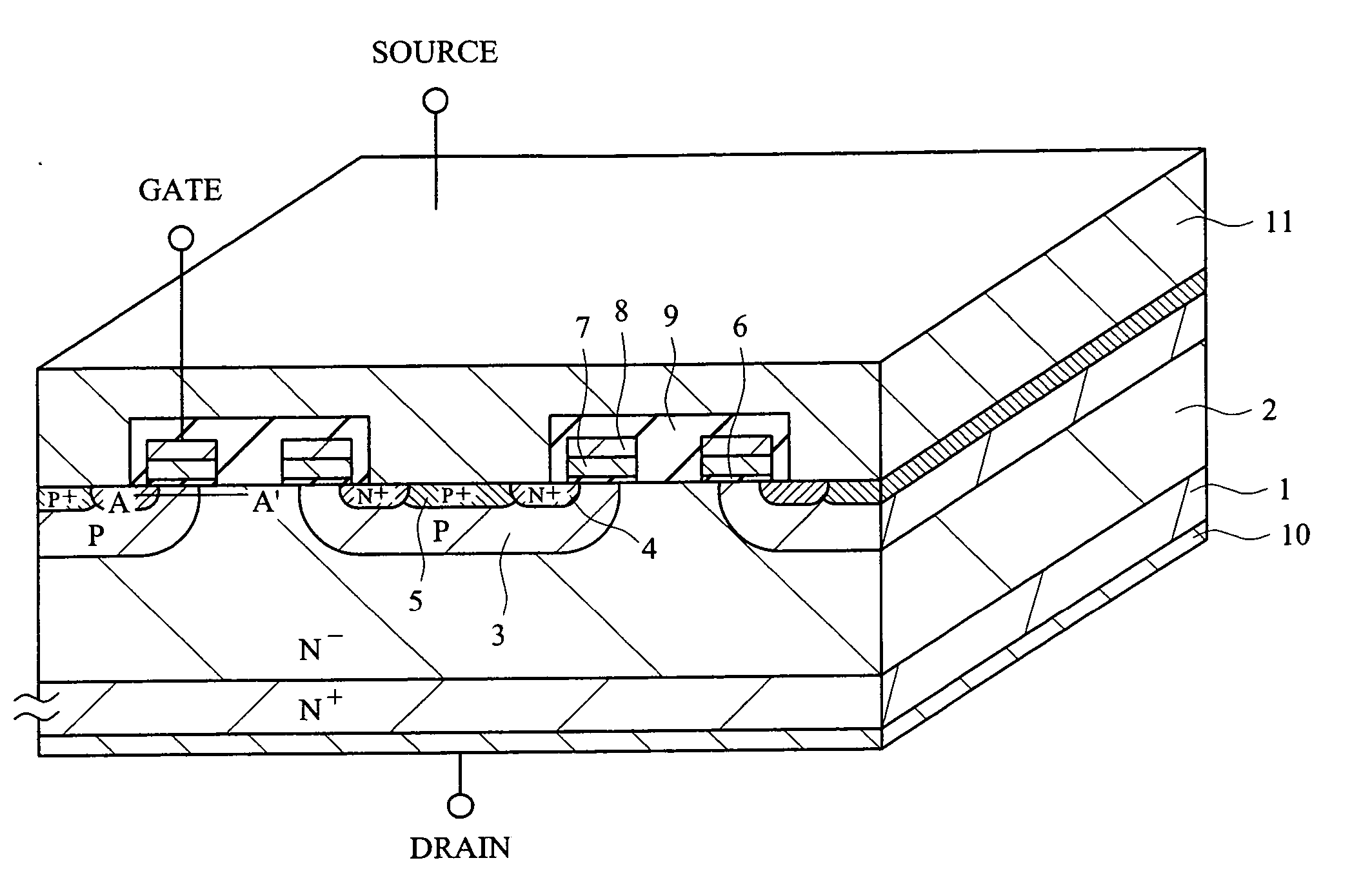
[0060] As shown in FIG. 1, the planar type MOSFET according to the first embodiment is a planar type N channel DMOSFET (Double-Diffused MOSFET), in which an N− epitaxial layer 2 is formed on an N+ substrate 1, and P channel layers 3, N+ source regions 4, and body contact regions 5 are formed in this N− epitaxial layer 2, and P type polysilicons 7 to be gate electrodes are formed thereon via gate insulating films 6. A part of the P type polysilicon 7 opposite to the JFET region between the P channel layers 3 is removed, and a tungsten silicide film 8 is formed on the P type polysilicon 7. The upper and side ...

second embodiment

[0076] The second embodiment of the present invention will be described with reference to FIG. 13. FIG. 13 is a diagram showing a cross-sectional structure of a planar type MOSFET according to the second embodiment of the present invention. The feature of FIG. 13 lies in that the N+ source region 4 and the body contact region 5 are alternatively arranged in a direction vertical to the gate. In such an arrangement, the cell pitch can be reduced without changing the dimensions of the JFET region and the ON-resistance can be reduced.

third embodiment

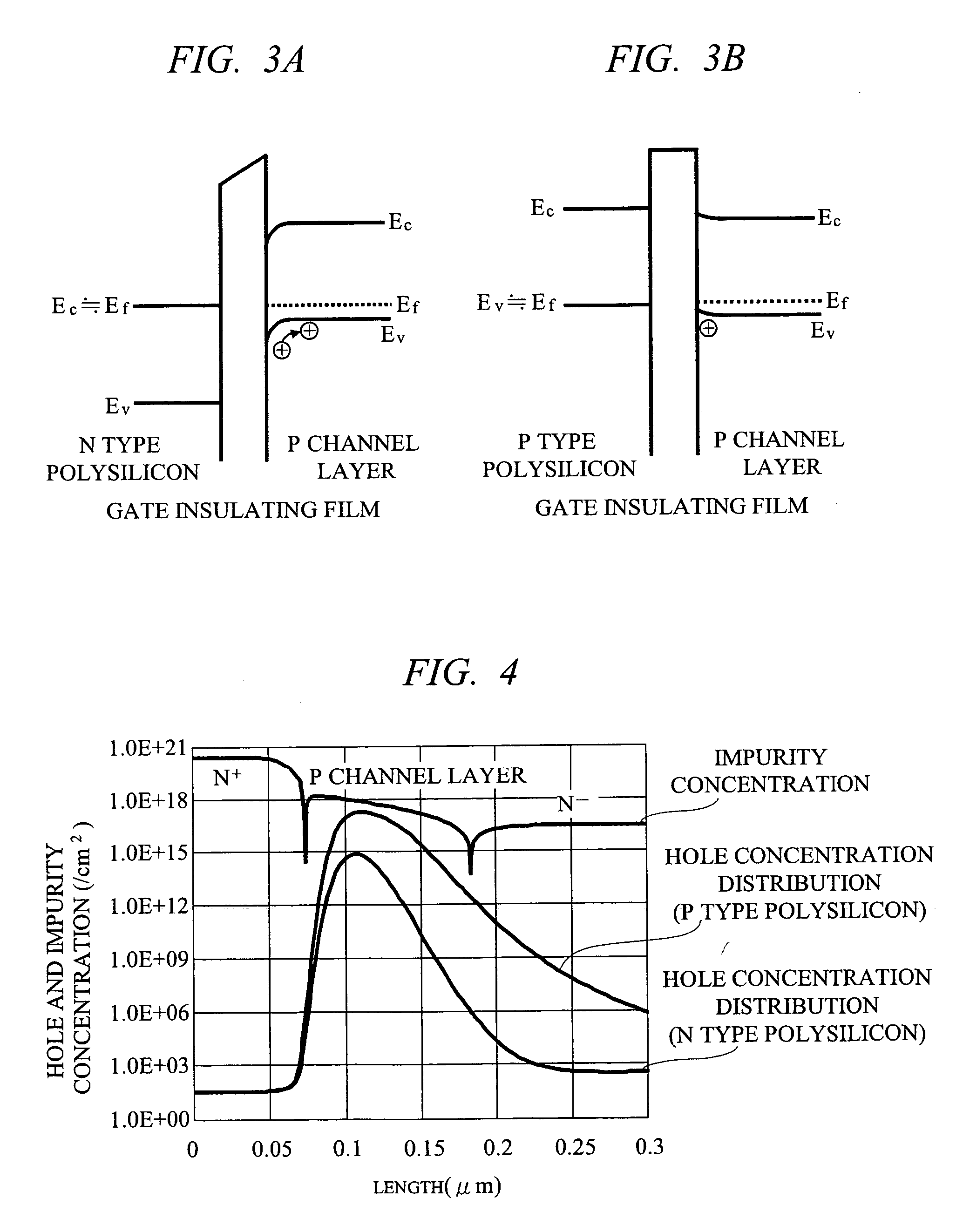
[0077] The third embodiment of the present invention will be described with reference to FIG. 14. FIG. 14 is a diagram showing a cross-sectional structure of a planar type MOSFET according to the third embodiment of the present invention. The feature of FIG. 14 lies in that an oxynitride film 14 is used for the gate insulating film. In the third embodiment, the P type polysilicon 7 is used for the gate electrode and boron (B) is used as an impurity thereof. It is known that the problem of the boron penetration occurs in the case of using an oxide film which is a normal gate insulating film. More specifically, when the thermal diffusion is performed at high temperature after the deposition of the P type polysilicon, boron in the P type polysilicon penetrates through the oxide film and reaches the semiconductor substrate. When the boron penetration occurs, the threshold voltage of the MOSFET becomes unstable.

[0078] It is known that the boron penetration described above can be prevent...


PUM


Abstract

A technology capable of realizing a MOSFET with low ON-resistance and low feedback capacitance, in which the punch through of a channel layer can be prevented even when the shallow junction of the channel layer is formed in a planar type MOSFET is provided. A P type polysilicon is used for a gate electrode in a planar type MOSFET, in particular, in an N channel DMOSFET.

Description

CROSS-REFERENCE TO RELATED APPLICATION [0001] The present application claims priority from Japanese Patent Application No. JP 2005-243547 filed on Aug. 25, 2005, the content of which is hereby incorporated by reference into this application. TECHNICAL FIELD OF THE INVENTION [0002] The present invention relates to a power MOSFET (Metal Oxide Semiconductor Field Effect Transistor). More particularly, it relates to a technology effectively applied to a structure and its manufacturing method suitable for achieving low ON-resistance and low feedback capacitance in a low withstand voltage power MOSFET with the withstand voltage of 100 V or lower and a power supply device using the power MOSFET. BACKGROUND OF THE INVENTION [0003] For example, current and frequency of a non-insulated DC / DC converter used in a power supply device of a desktop PC, a note PC, a game machine and others have been increasing due to the demands for higher current for CPU (Central Processing Unit) and MPU (Micro Pr...

Claims


Application Information

Patent Timeline
Patent Type & Authority Applications(United States)
IPC IPC(8): H01L29/76
CPCH01L29/0634H01L29/0696H01L29/086H01L29/0878H01L29/1095H01L29/402H01L29/7806H01L29/42372H01L29/4916H01L29/4933H01L29/518H01L29/66712H01L29/7802H01L29/42368
Inventor SHIRAISHI, MASAKIIWASAKI, TAKAYUKIMATSUURA, NOBUYOSHINAKAZAWA, YOSHITOKACHI, TSUYOSHI
Owner RENESAS TECH CORP
Why Eureka
Try Eureka