Piezoelectric member, piezoelectric member element, liquid discharge head in use thereof, liquid discharge apparatus and method of manufacturing piezoelectric member

a piezoelectric and piezoelectric technology, applied in the direction of piezoelectric/electrostrictive device material selection, device material selection, printing, etc., can solve the problems of insufficient production, difficult production, and 0.1 to 0.15%, and achieve stable piezoelectric characteristics and good driving response

Inactive Publication Date: 2007-03-01
CANON KK
View PDF20 Cites 35 Cited by
  • Summary
  • Abstract
  • Description
  • Claims
  • Application Information

AI Technical Summary

Benefits of technology

[0009] The present invention has been attained for the above-described problems and it is an object thereof to provide a piezoelectric member and a piezoelectric member element with good driving response in a high-frequency region. In addition, it is another object to provide a method of manufacturing piezoelectric member which will enable reduction in loads for circuit design such as a wiring resistance limit value, a driving power supply capacity of the piezoelectric member element and the like and which can maintain stable piezoelectric characteristics even under any use environments.

Problems solved by technology

However, a strain amount thereof is around 0.1 to 0.15% even at maximum and may not be called sufficient in case of being used as a piezoelectric actuator and the like.
However, for example, a MEMS piezoelectric actuator, development of which is being proceeded enthusiastically in recent years, is finely structured and therefore production thereof is very difficult since uniaxial crystal is required to be made into thin pieces for junction in case of using uniaxial crystal material which has been caused to grow in a bulk state as described in Japanese Patent No. 3397538.
Accordingly, supply of electric power to drive it gives rise to phase delay of supply power due to relationship with wire resistance, an issue of delay in drive response to high frequency drive accompanied thereby, an issue such as tendency to larger driving power supply capacity and the like.
Therefore the issue of delay in drive response to high frequency drive and the issue of requirement of larger driving power supply capacity are significant problems.
Accordingly, a case of application into the ink jet head gives rise to an issue that stable discharge performance cannot be maintained under various use environments and such environments that will increase temperature of a piezoelectric member element due to continued use.

Method used


Image

  • Piezoelectric member, piezoelectric member element, liquid discharge head in use thereof, liquid discharge apparatus and method of manufacturing piezoelectric member
  • Piezoelectric member, piezoelectric member element, liquid discharge head in use thereof, liquid discharge apparatus and method of manufacturing piezoelectric member
  • Piezoelectric member, piezoelectric member element, liquid discharge head in use thereof, liquid discharge apparatus and method of manufacturing piezoelectric member

Examples


example 1

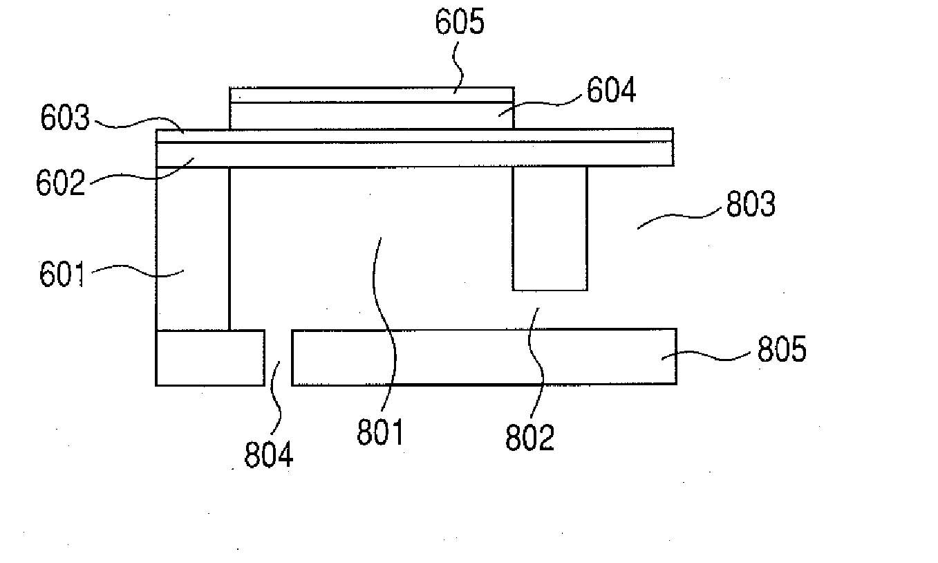
[0087]FIG. 6 is a sectional diagram of configuration of a film piezoelectric member formed on a substrate.

[0088] Reference numeral 600 denotes a substrate for forming a film piezoelectric member. Reference numeral 601 denotes Si(100) substrate (t=200 μm, and stabilized zirconia (YSZ) is brought into reactive sputter film-forming at a substrate temperature of 800° C. in an Ar / O2 atmosphere so as to form film of the vibration plate 602 of (100)YSZ epitaxial film of 3 μm. Next, as the lower electrode 603, strontium ruthenate (SrRuO3(=SRO)) is brought into reactive sputter film-forming at a substrate temperature of 600° C. in an Ar / O2 atmosphere so as to form film of the lower electrode 603 of (001)SRO epitaxial film of 300 nm. Thereby, the substrate 600 that can derive a film piezoelectric member with epitaxial growth is prepared.

[0089] Next, a method of forming a film piezoelectric member 604 will be described.

[0090]FIG. 7 is a schematic diagram of an RF magnetron sputter apparatus...

example 2

[0115] Except that a temperature drop was carried out continuously from 600° C. for ten minutes to reach 25° C. after forming a film piezoelectric member 604, a piezoelectric member element for measuring relative dielectric constants and an ink jet head were produced likewise Example 1 to assess their performance. Table 1 shows results thereof.

[0116] Here, it was confirmed with X-ray structure analysis that the formed film piezoelectric member 604 was uniaxial crystal and an outcome of composition analysis by ICP optical emission spectrometry turned out to be Pb / Mg / Nb / Ti=110 / 43.3 / 26.7 / 30.

example 3

[0117] A sintered member with composition proportion of Pb / Zn / Nb / Ti=120 / 30.3 / 60.7 / 9 was prepared as the source material target 702 and the temperature to be retained in a balanced state on the temperature at the time of a temperature drop after forming the film piezoelectric member 604 was set to 400° C. (Step 2). Otherwise, likewise Example 1, the film piezoelectric member 604 was derived.

[0118] As described above, X-ray structure analysis was carried out to confirm that the film piezoelectric member 604 was film having undergone epitaxial growth and was uniaxial crystal.

[0119] In addition, composition analysis by ICP optical emission spectrometry was carried out to note that a composition of the film piezoelectric member 604 was Pb / Zn / Nb / Ti=108 / 30.3 / 60.7 / 9.

[0120] Moreover, an ink jet head was produced likewise Example 1 to assess its performance. Table 1 shows results thereof.


PUM

PropertyMeasurementUnit
temperatureaaaaaaaaaa
thicknessaaaaaaaaaa

Abstract

A piezoelectric member of uniaxial crystal or uniaxial crystal and the piezoelectric member has perovskite type oxide described to be ABO3 in a general formula with a main component of the A being Pb and a main component of the B containing at least three kinds of elements selected from the group consisting of Mg, Zn, Sc, In, Yb, Ni, Nb, Ti and Ta and film thickness of the piezoelectric member is not less than 1 μm and not more than 10 μm and the piezoelectric member fulfills a predetermined conditions on relative dielectric constant or Curie temperature.

Description

BACKGROUND OF THE INVENTION [0001] 1. Field of the Invention [0002] The present invention relates to a piezoelectric member, a piezoelectric member element, an actuator in use thereof and a liquid discharge head (an ink jet head) as well as a method of manufacturing the piezoelectric member. [0003] 2. Description of the Related Art [0004] Metal oxide ceramics consisting of PZT(Pb(Zr,Ti)O3) system are generally known as a piezoelectric member. These PZT system ceramics have excellent piezoelectric characteristics and are widely used for a piezoelectric actuator, a piezoelectric ignition element, a piezoelectric buzzer, a piezoelectric transformer and the like. However, a strain amount thereof is around 0.1 to 0.15% even at maximum and may not be called sufficient in case of being used as a piezoelectric actuator and the like. In recent years, for a purpose of obtaining further piezoelectric characteristics or a large amount of strain, relaxor material is being considered and, for exa...

Claims


Application Information

Patent Timeline
Patent Type & Authority Applications(United States)
IPC IPC(8): B41J2/045
CPCH01L41/18B41J2/14233H10N30/85H10N30/8548
Inventor AOKI, KATSUMIMATSUDA, TAKANORIIFUKU, TOSHIHIRO
Owner CANON KK
Why Eureka
Try Eureka