Methods of forming semiconductor constructions and capacitors

a technology of capacitors and semiconductors, applied in the direction of capacitors, semiconductor devices, electrical equipment, etc., can solve the problem of weak structural strength of containers

Inactive Publication Date: 2007-03-01
MICRON TECH INC
View PDF10 Cites 84 Cited by
  • Summary
  • Abstract
  • Description
  • Claims
  • Application Information

AI Technical Summary

Problems solved by technology

Unfortunately, exposure of both the interior and exterior surfaces of a container having a high aspect rat

Method used


Image

  • Methods of forming semiconductor constructions and capacitors
  • Methods of forming semiconductor constructions and capacitors
  • Methods of forming semiconductor constructions and capacitors

Examples


Embodiment Construction

[0036] This disclosure of the invention is submitted in furtherance of the constitutional purposes of the U.S. Patent Laws “to promote the progress of science and useful arts” (Article 1, Section 8).

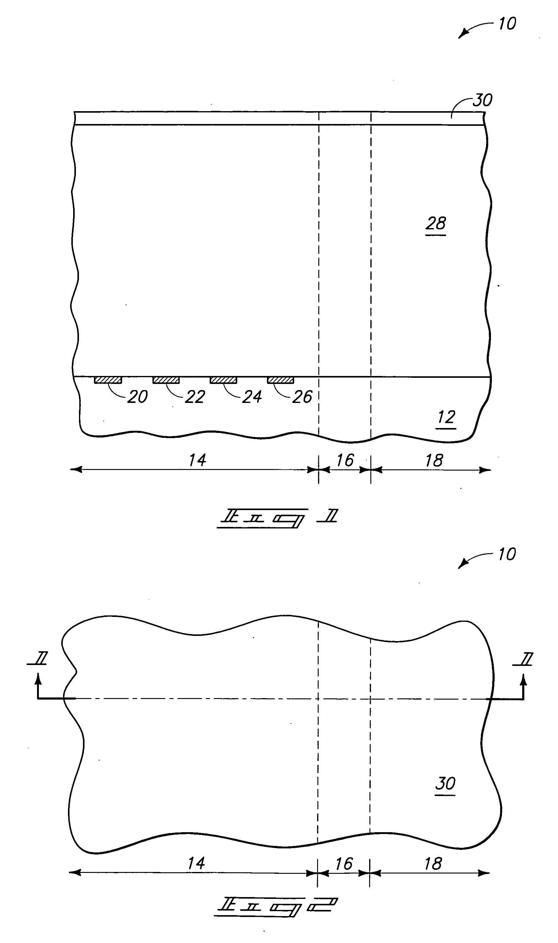
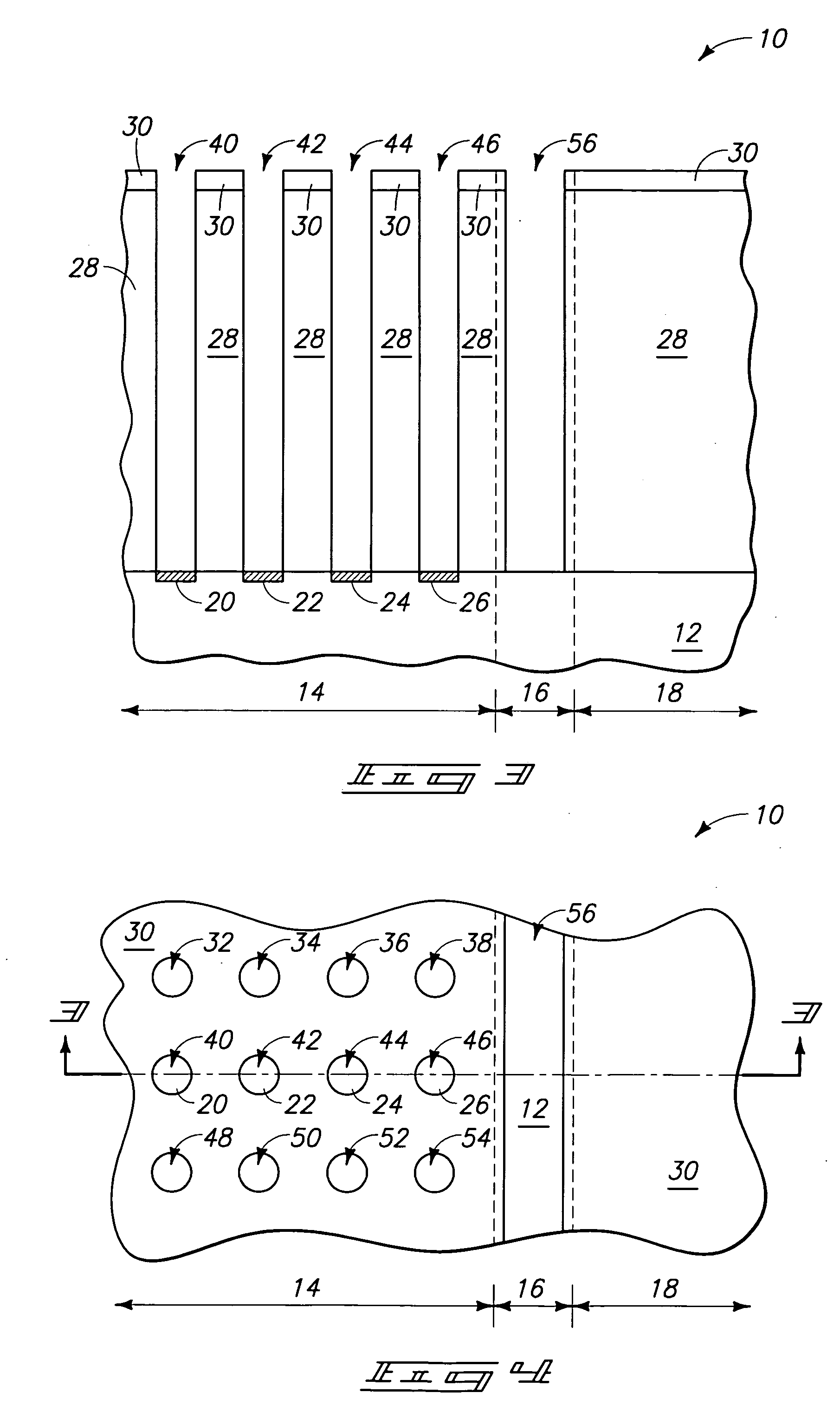
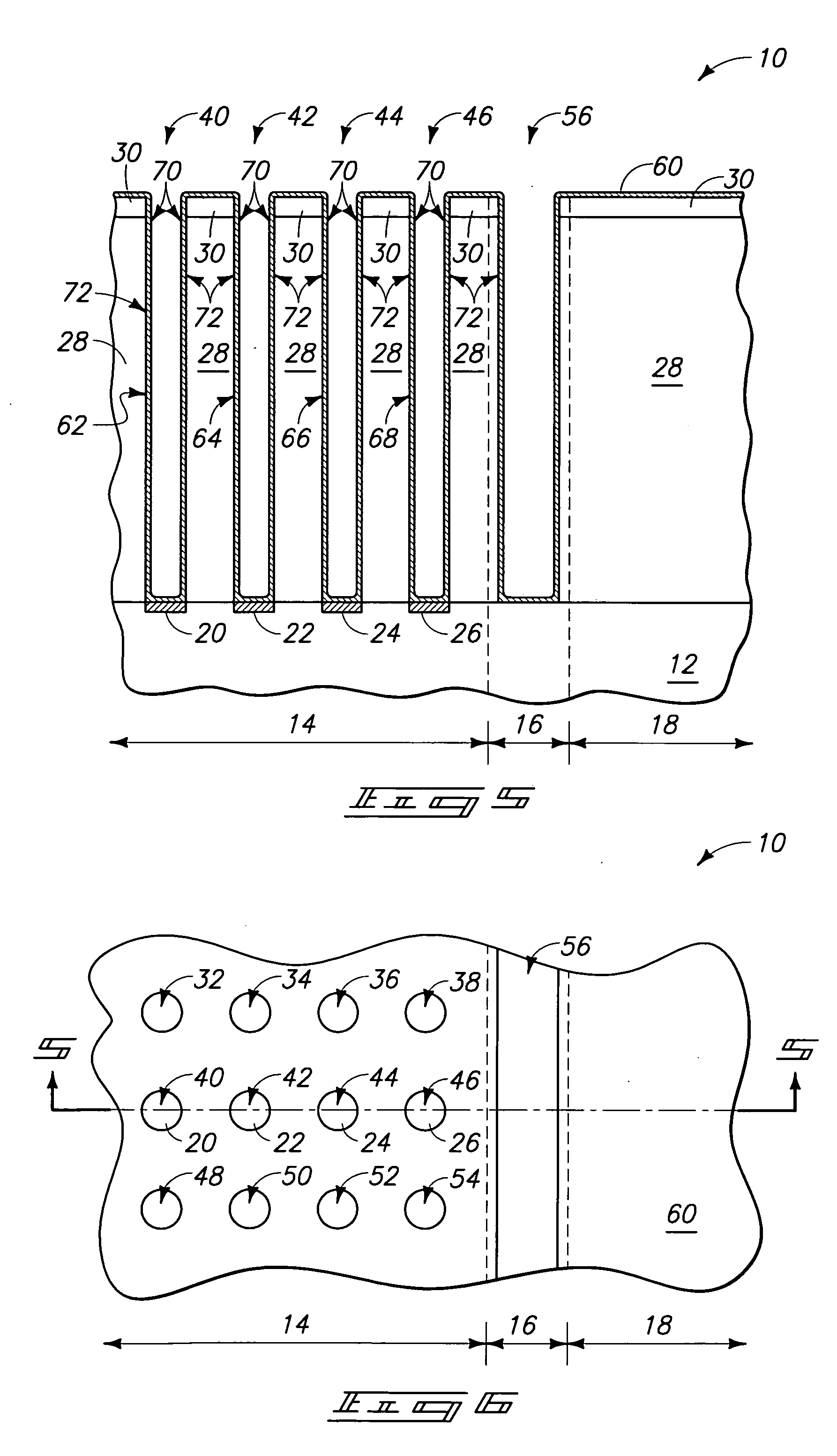
[0037] The invention includes methodology for forming container capacitors. In typical processing, a semiconductor wafer will have a memory array region where capacitors are to be formed. It can be desired to etch sacrificial silicon-containing material from the memory array region, while avoiding formation of conductive whiskers from storage node material exposed to the etch. Methodology of the present invention can include dispersal of phosphoric acid in the etching solution utilized to remove the silicon to alleviate the formation of the conductive whiskers. The invention can additionally, or alternatively, include methodology for removing any whiskers that have formed.

[0038] Various aspects of the invention are described below with reference to FIGS. 1-25.

[0039] Referring to FIG. ...


PUM


Abstract

The invention includes methods in which silicon is removed from titanium-containing container structures with an etching composition having a phosphorus-and-oxygen-containing compound therein. The etching composition can, for example, include one or both of ammonium hydroxide and tetra-methyl ammonium hydroxide. The invention also includes methods in which titanium-containing whiskers are removed from between titanium-containing capacitor electrodes. Such removal can be, for example, accomplished with an etch utilizing one or more of hydrofluoric acid, ammonium fluoride, nitric acid and hydrogen peroxide.

Description

TECHNICAL FIELD [0001] The invention pertains to methods of forming semiconductor constructions, and in particular aspects pertains to methods of forming capacitors associated with semiconductor constructions. BACKGROUND OF THE INVENTION [0002] Capacitors continue to have increasing aspect ratios in higher generation integrated circuitry fabrication. For example, dynamic random access memory (DRAM) capacitors now have elevations of from 2 to 3 microns, and widths of about 0.1 micron. Further, it is a continuing goal to increase the density of semiconductor devices, with a corresponding goal to reduce the footprint associated with individual devices. As the packing density of capacitors becomes increasingly greater, the available surface area for capacitance decreases. [0003] A common type of capacitor is a so-called container device, which is typically in cylindrical form. One of the electrodes of such device is shaped as a container, and subsequently dielectric material and another...

Claims


Application Information

Patent Timeline
IPC IPC(8): H01L21/20H01L21/302
CPCH01L21/30604H01L28/91H01L27/10894H01L27/10852H10B12/09H10B12/033
Inventor RAGHU, PRASHANT
Owner MICRON TECH INC
Why Eureka
Try Eureka