
Coherent light source and optical device

Inactive Publication Date: 2007-03-08
PANASONIC CORP
View PDF13 Cites 17 Cited by
  • Summary
  • Abstract
  • Description
  • Claims
  • Application Information

AI Technical Summary

Benefits of technology

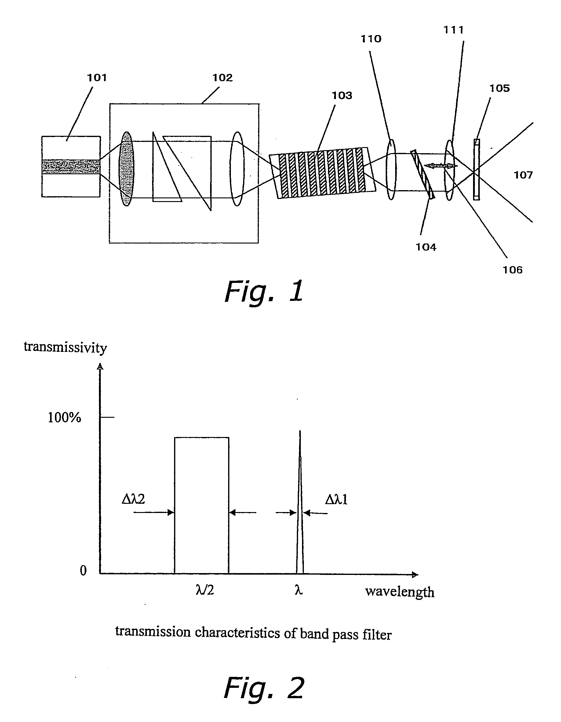
[0009] In view of this, the coherent light source of the present invention comprises a light source, a wavelength conversion element that converts part of a fundamental wave emitted from the light source into a higher harmonic wave, and a wavelength selecting filter that has narrow-band transmission characteristics with respect to the part of the fundamental wave not converted into the higher harmonic wave, and has transmission characteristics with respect to the higher harmonic wave. The part of the fundamental wave emitted from the wavelength conversion element but not converted into the higher harmonic wave is fed back to the light source by the wavelength selecting filter, and the higher harmonic wave is emitted to the outside after passing through the wavelength selecting filter. This affords a short-wavelength light source that has high output and is stable, and is extremely well suited to mass production.
[0030] By endowing a wavelength selecting filter with higher harmonic wave transmission characteristics as above, an optical system can be simplified, made more compact, and stabilized. Also, the optical system itself can be developed for direct coupling systems that are much smaller in size. This in turn affords a short-wavelength light source that has high output and is stable, and is extremely well suited to mass production.

Problems solved by technology

Nevertheless, problems with the above conventional methods were that they entailed so many optical components, and the optical system was complicated, making it difficult to stabilize an optical system and reduce its size.
Furthermore, since the optical axis at which a higher harmonic wave was generated was at an angle to the optical axis of the fundamental wave incident light, another problem was difficulty in adjusting the optical axis.
With this method, though, there is a decrease of over 20% in the fundamental wave whose wavelength is converted, and the output of higher harmonic waves decreases by more than 40%, which poses problems in terms of raising output.

Method used


Image

  • Coherent light source and optical device
  • Coherent light source and optical device
  • Coherent light source and optical device

Examples


first embodiment

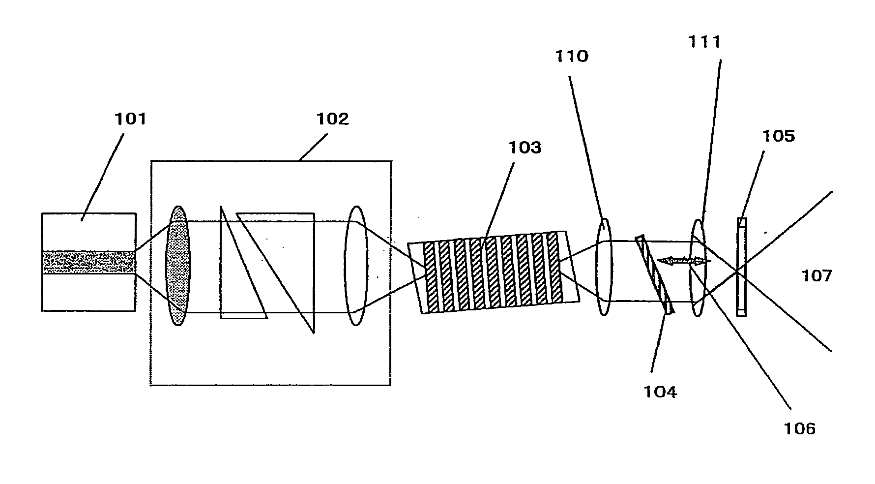
[0061]FIG. 1 shows an example of the structure of the coherent light source of the present invention. In the example shown here, a wavelength selecting filter is constituted by a band pass filter and a dichroic mirror. The wavelength selecting filter is a confocal optical system, and the dichroic mirror is installed in the focal plane of the confocal optical system. The coherent light source comprises a semiconductor laser 101, a focusing optical system 102, a wavelength conversion element 103, a collimating lens 110, a band pass filter 104, a focusing lens 111, and a dichroic mirror 105.

[0062] The band pass filter 104 is composed of a dielectric multilayer film, and transmits only certain wavelengths with respect to the fundamental wave of the semiconductor laser 101. This will be described in further detail below. The dichroic mirror 105 is designed so as to reflect fundamental waves and transmit at least 95% of higher harmonic waves.

[0063] Next, the coherent light source of the...

second embodiment

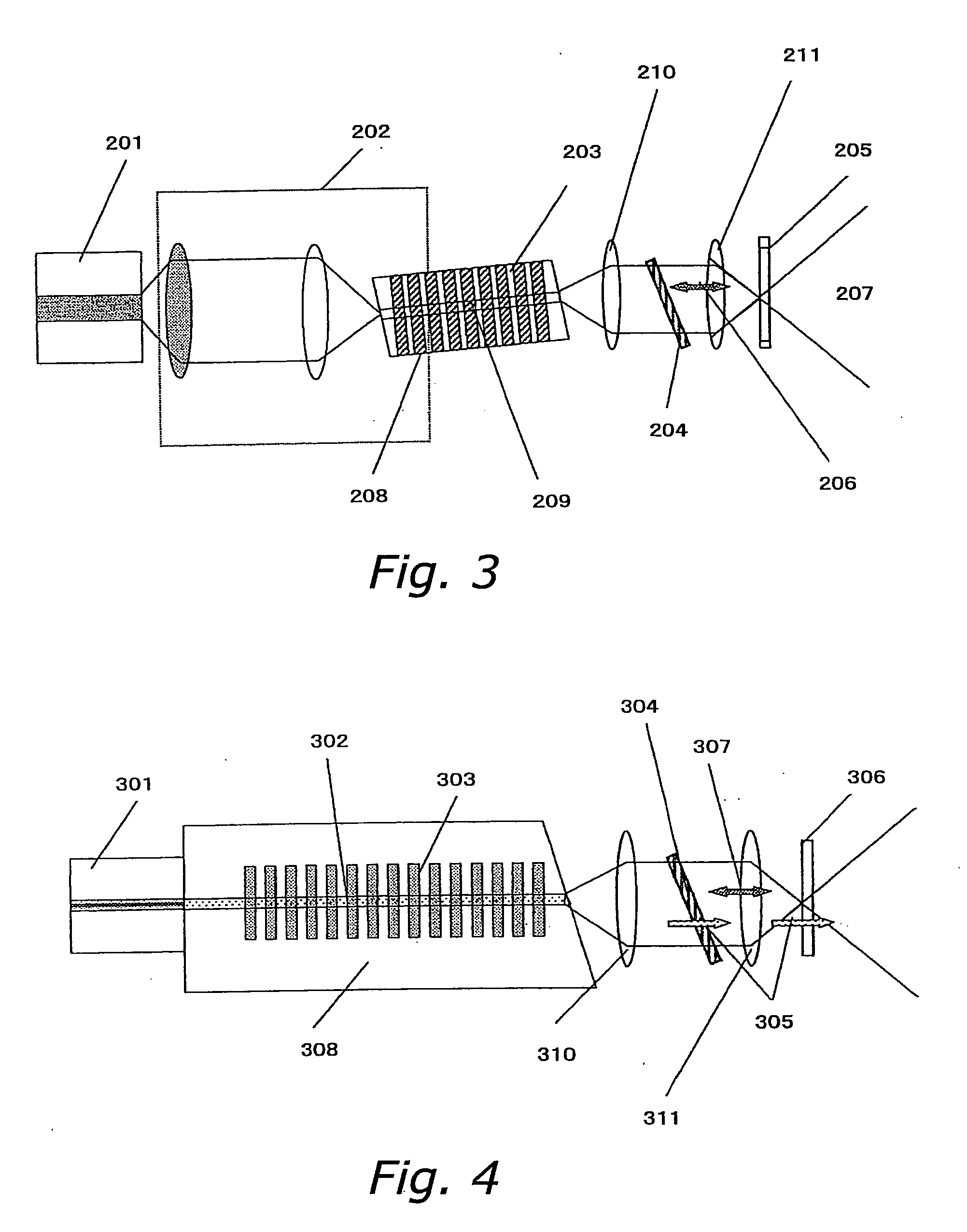
[0077] We will now describe an example of applying the structure of the present invention to a wavelength conversion element that makes use of an optical waveguide. In FIG. 3, a wavelength conversion element 203 comprises a periodic polarization inverter 208 and an optical waveguide 209. The fundamental wave that exits a semiconductor laser 201 is focused on the optical waveguide 209. The fundamental wave that propagates through the optical waveguide 209 is subjected to wavelength conversion by the periodic polarization inverter 208, and becomes a higher harmonic wave. Using the optical waveguide 209 results in a high conversion efficiency of about 50%, and a 200 mW higher harmonic wave (wavelength 490 nm) is obtained from the semiconductor laser 201, which has a wavelength of 980 nm and an output of 500 mW. This constitution simplifies and stabilizes the optical system, and yields a coherent light source that is compact and stable.

[0078] Furthermore, with a waveguide type, the dir...

third embodiment

[0085] Here, we will describe a laser display as an example of an optical device that makes use of the coherent light source of the present invention.

[0086] With a laser display, a display of high color reproducibility can be achieved by using an RGB laser. High-output red semiconductor lasers have been developed as laser light sources. An increase in output has not been achieved with blue, however, and the very formation of a semiconductor laser is difficult with green. In view of this, it is necessary to use blue and green light sources that utilize wavelength conversion. In the coherent light source of the present invention, since a wide stripe semiconductor laser can be used, high-output blue and green light can be obtained by combining with a wavelength conversion element. For blue output, blue light of 440 nm can be obtained by subjecting a semiconductor laser of 880 nm to wavelength conversion, and for green output, green light of 530 nm can be obtained by subjecting a semic...


PUM


Abstract

It is easy to increase output with a wide stripe laser, but the lateral mode is a multimode, and the coupling efficiency is low with a single-mode fiber or a single-mode waveguide, creating problems in terms of increasing output. To solve these problems, the light emitted from a wide stripe semiconductor laser is passed through a mode converter and a wavelength selecting filter, then fed back to the active layer of the semiconductor laser, which fixes the oscillation mode of the semiconductor laser to single mode.

Description

TECHNICAL FIELD [0001] The present invention relates to a coherent light source that makes use of a wavelength conversion element, and to an optical device. BACKGROUND ART [0002] Wavelength conversion elements featuring a semiconductor laser can be made smaller and have higher output, and the wavelength can be shortened by utilizing wavelength conversion to a higher harmonic wave. On the other hand, the wavelength tolerance for a wavelength conversion element to convert wavelengths at high efficiency is generally extremely narrow, which means that the oscillation wavelength of the semiconductor laser has to be stabilized to stabilize the output. [0003] Providing optical feedback to the semiconductor laser has been proposed as a way to solve this problem. The waveguide mode of a semiconductor laser can be controlled by external optical feedback. For instance, it has been indicated that the oscillation wavelength of a semiconductor laser can be fixed by using a narrow-band wavelength ...

Claims


Application Information

Patent Timeline
IPC IPC(8): H01S3/10G02F1/35G02F1/37H01S3/00H01S3/06H01S3/08H01S3/109
CPCG02F2001/3503H01S3/005H01S3/109H01S3/08004H01S3/08059H01S3/0604G02F1/3503
Inventor MIZUUCHI, KIMINORI
Owner PANASONIC CORP
Learn More