Scanning electron microscope

a scanning electron microscope and electron microscope technology, applied in the field of scanning electron microscope, can solve the problems of complex device control, low throughput, and inability to observe on the spot, and achieve the effects of reducing the potential gradient, high-speed relaxation and stabilizing the electrification, and stabilizing the s/n ratio and contras

Inactive Publication Date: 2007-03-15
HITACHI HIGH-TECH CORP
View PDF4 Cites 18 Cited by
  • Summary
  • Abstract
  • Description
  • Claims
  • Application Information

AI Technical Summary

Benefits of technology

[0028] According to the device configuration of the present invention, it becomes possible to eliminate the potential gradient on an insulating-substance sample surface, and to perform high-speed relaxation and stabilization of the electrification induced when a charged particle beam is irradiated onto the insulating-substance sample. Even in the high magnification under which the length-measurement is performed, it becomes possible to stabilize the S/N ratio and contrast, and to eliminate the beam drift as well. As a result, it becomes possible to perform the ...

Problems solved by technology

Any of the above-cited techniques and units, however, has the following drawbacks: An on-the-spot observation is impossible to make, the throughput is low, the device control is complicated, the resolution is low, the maintenance is difficult and the period is short, a photosensitive material such as resist is unsuitable therefor, and the like.
Accordingly, since the effect of the sample stage lacks in the conventional techniques, it is impossi...

Method used


Image

  • Scanning electron microscope
  • Scanning electron microscope
  • Scanning electron microscope

Examples


Embodiment Construction

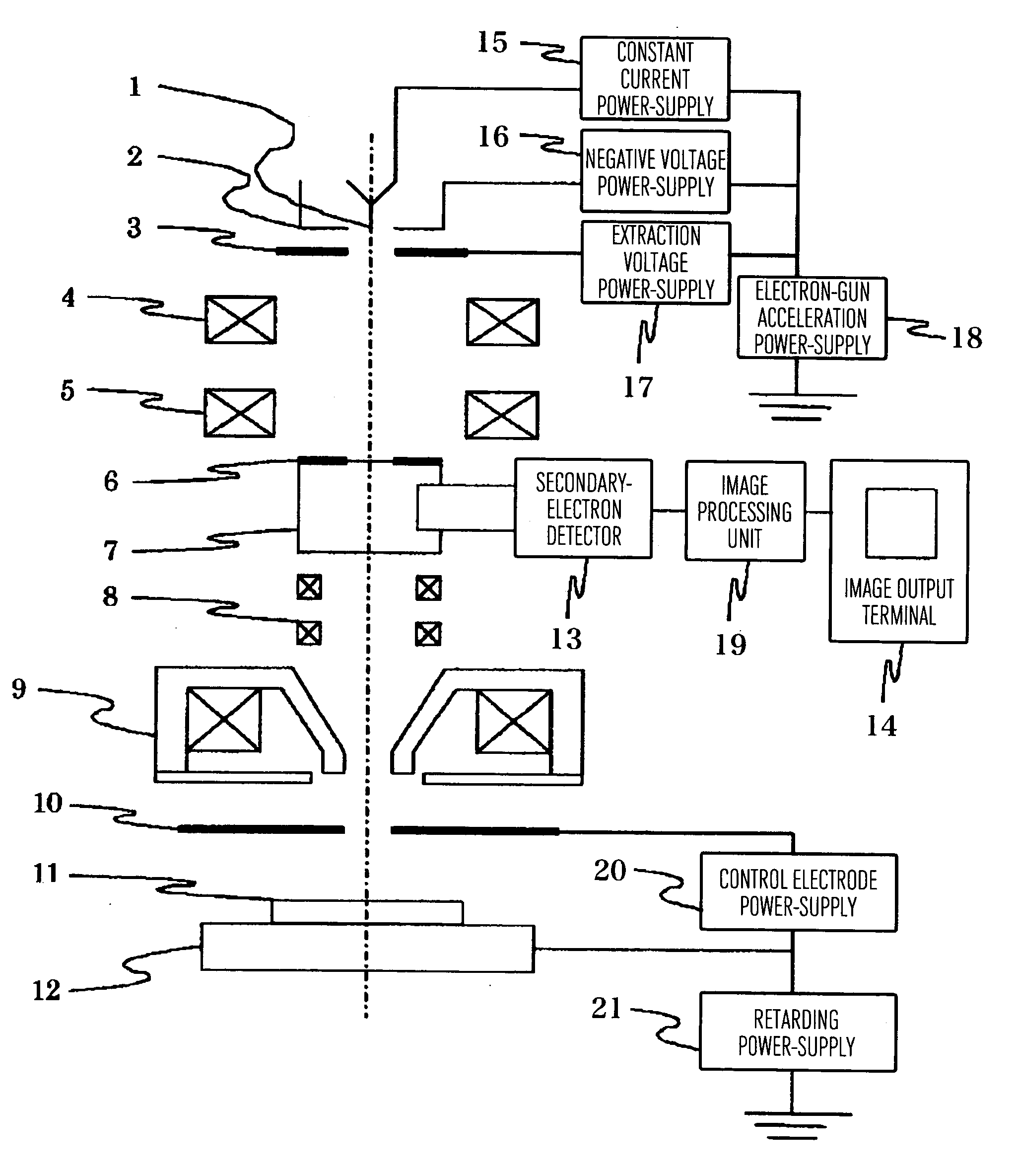
[0030] First, referring to FIG. 1, the explanation will be given below concerning a representative embodiment of the present invention. The present embodiment is of the basic configuration of a scanning electron microscope (SEM) which uses the retarding method. The whole or a part of configuration components 1 to 12 of the present embodiment is contained within a vacuum container. The electron source 1 is the so-called “Schottky electron source”, i.e., an electron source where zirconium oxide is coated and diffused on a needle-shaped-machined tungsten thereby to decrease the work function of an electron emission portion at the electron source front-end. The electron source 1 is heated at a proper temperature by a constant current power-supply 15 which is kept floating over an electron-gun acceleration power-supply 18 for applying an electron-beam initial acceleration voltage −3 kV to the electron source. Then, electron emission is performed at an extraction electrode 3 to which an e...


PUM


Abstract

An object of the invention is to reduce the beam drift in which the orbit of the charged particle beam is deflected by a potential gradient generated by a nonuniform sample surface potential on a charged-particle-beam irradiation area surface, the nonuniform sample surface potential being generated by electrification made when observing an insulating-substance sample using a charged particle beam.
Energy of the charged particle beam to be irradiated onto the sample is set so that generation efficiency of secondary electrons generated from the sample becomes equal to 1 or more. A flat-plate electrode (26) is located in such a manner as to be directly opposed to the sample. Here, the flat-plate electrode is an electrode to which a voltage can be applied independently, and which is equipped with a hole through which a primary charged particle beam can pass. Furthermore, a voltage can be applied independently to a sample stage (12) on which the sample is mounted. Here, the sample stage's surface directly opposed to the sample is formed into a planarized structure with no projections and depressions thereon. Also, diameter D of the hole provided in the flat-plate electrode (26) and distance L between the flat-plate electrode (26) and the sample are set such that a relation of D/L≦1.5 is satisfied.

Description

TECHNICAL FIELD [0001] The present invention relates to a control technique for controlling electrification. This electrification turns out to become a problem when observing an insulating-substance sample in devices which use a charged particle beam as the probe. Examples of such devices are a scanning electron microscope (SEM) and a focused-ion-beam (FIB) machining and observation device. Also, it is highly likely that electric charges will be accumulated on glass-substrate samples by irradiation with the charged particle beam. Examples of such glass-substrate samples are a reticle (i.e., mask) and a quartz wafer. Accordingly, in particular, the present invention relates to a technique for allowing a pattern configured on the glass-substrate samples to be stably length-measured using the charged particle beam devices. BACKGROUND ART [0002] In the SEM observation of an insulating-substance composed sample by using a charged particle beam, the main object and concern has been placed...

Claims


Application Information

Patent Timeline
IPC IPC(8): G21K7/00
CPCH01J37/026H01J37/28H01J2237/2817H01J2237/12H01J2237/0044
Inventor ARAI, NORIAKIEZUMI, MAKOTOOSE, YOICHI
Owner HITACHI HIGH-TECH CORP
Why Eureka
Try Eureka