Epitaxially coated silicon wafer and method for producing epitaxially coated silicon wafers

a technology of epitaxial coating and silicon wafers, which is applied in the direction of chemically reactive gases, crystal growth processes, polycrystalline material growth, etc., can solve the problems of 25% of epitaxially coated silicon wafers not meeting local flatness requirements, and the local flatness of epitaxially coated silicon wafers is significantly poorer. , to achieve the effect of high yield

Active Publication Date: 2007-03-22
SILTRONIC AG
View PDF23 Cites 31 Cited by
  • Summary
  • Abstract
  • Description
  • Claims
  • Application Information

AI Technical Summary

Benefits of technology

[0026] Therefore, an object of the invention was to provide a method for epitaxially coating silicon wafers which, on the one hand makes a higher yield possible, and on the other hand makes it possible to produce epitaxially coated silicon wafers with a low edge roll-off. These and ot...

Problems solved by technology

It has been shown in the prior art that some of the epitaxially coated silicon wafers have a significantly poorer local flatness in the edge region.
Thus, by way of example, if an etching treatment of the susceptor is carried out after 4 epitaxial depositions, it may be observed that in each case one of the silicon wafers that are epitaxially coated between two susceptor treatments exhibits a significantly poorer local flatness in the edge region, which in this case...

Method used


Image

  • Epitaxially coated silicon wafer and method for producing epitaxially coated silicon wafers
  • Epitaxially coated silicon wafer and method for producing epitaxially coated silicon wafers
  • Epitaxially coated silicon wafer and method for producing epitaxially coated silicon wafers

Examples


example

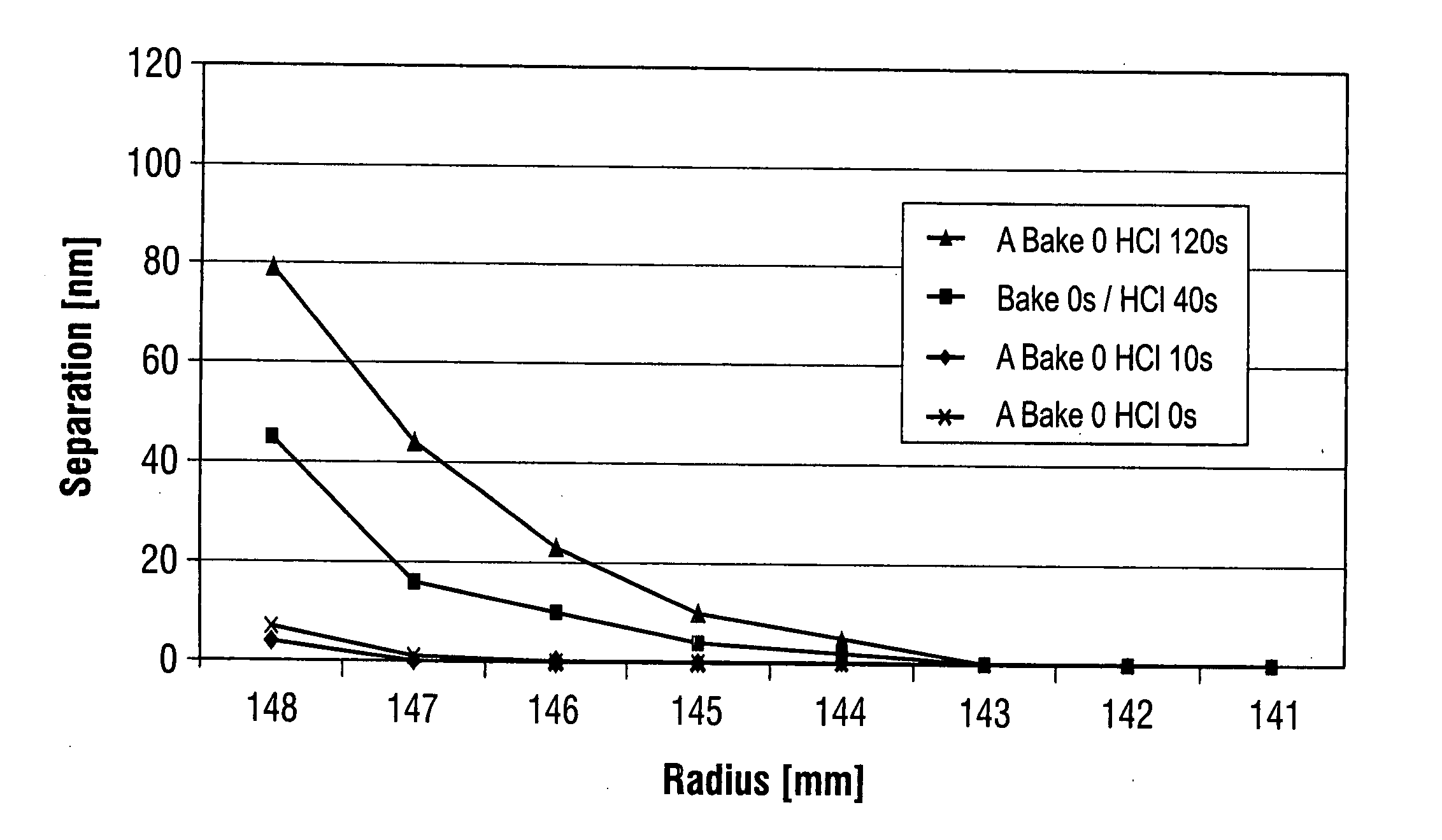
[0065] Determination of the initial geometry of a concavely polished silicon wafer prior to pretreatment / epitaxy resulted in the following R30 values: an R30-1 mm of −120 nm, an R30-2 mm of 50 nm and an R30-3 mm of −30 nm.

[0066] This concavely polished silicon wafer was epitaxially coated according to the invention, the following process parameters having been chosen: heating of the susceptor without a substrate to 1100° C.; H2 bake pretreatment with H2 flow rate of 60 slm and treatment duration of 20 s; HCl etching treatment with H2 flow rate of 50 slm and treatment duration of 60 s; epitaxial deposition by means of TCS at a deposition temperature of 1120° C., a TCS flow rate of 17 slm, and deposition duration of 63 sec. For the epitaxially coated silicon wafer, a significantly better value of −7 nm results for the R30-1 mm edge roll-off parameter. At a distance of 2 mm and 3 mm from the edge, the curve averaged over all the radial cross sections lies above the reference line. The...


PUM


Abstract

Epitaxially coated silicon wafers, are produced by epitaxially coating a multiplicity of wafers polished at least on their front sides, successively and individually in an epitaxy reactor, by placing a silicon wafer on a susceptor, pretreating under a hydrogen atmosphere followed by addition of an etching medium to the hydrogen atmosphere, coating epitaxially on the polished front side and removing the water from the epitaxy reactor. The susceptor is then heated, in each case, to a temperature of at least 1000° C. under a hydrogen atmosphere, and furthermore an etching treatment of the susceptor and a momentary coating of the susceptor with silicon are effected after a specific number of epitaxial coatings. Silicon wafers characterized by a parameter R30-1 mm of −10 nm to +10 nm, determined at a distance of 1 mm from the edge of the silicon wafer are produced.

Description

BACKGROUND OF THE INVENTION [0001] 1. Field of the Invention [0002] The invention relates to an epitaxially coated silicon wafer and a method for producing epitaxially coated silicon wafers. [0003] 2. Background Art [0004] Epitaxially coated silicon wafers are suitable for use in the semiconductor industry, in particular for the fabrication of large scale integrated electronic components such as microprocessors or memory chips. Starting materials (substrates) with stringent requirements are required for modern microelectronics, for example global and local flatness, edge geometry, thickness distribution, single-side-reference local flatness (nanotopology) and freedom from defects. [0005] According to the prior art, a silicon wafer can be produced by a process sequence of separating a single crystal of silicon into wafers, rounding the mechanically sensitive edges, carrying out an abrasive step such as grinding or lapping followed by a polishing. EP 547894 A1 describes a lapping meth...

Claims


Application Information

Patent Timeline
IPC IPC(8): C30B23/00C30B25/00C30B28/12C30B28/14
CPCC30B29/06C30B25/02H01L21/20
Inventor SCHAUER, REINHARDHAGER, CHRISTIAN
Owner SILTRONIC AG
Why Eureka
Try Eureka