Active load arrangement

a technology of active load and arrangement, which is applied in the direction of pulse generators, pulse techniques, instruments, etc., can solve the problems of high voltage at circuit breaking, and high impedance for active load arrangemen

Inactive Publication Date: 2007-03-22
TELEFON AB LM ERICSSON (PUBL)
View PDF6 Cites 3 Cited by
  • Summary
  • Abstract
  • Description
  • Claims
  • Application Information

AI Technical Summary

Benefits of technology

[0006] More in detail, the active load arrangement comprises a voltage-controlled transistor called Metal Oxide Semiconductor Field Effect Transistor, MOSFET, having a source, a gate and a drain. The drain is connected to an input of the arrangement associated with an output of the object under test. A resistor is connected between the gate and the drain. An inductance is connected between the source and an output of the arrangement associated with an input of the object under test. A capacitance is connected between the gate and the arrangement output.
[0007] One advantage with the invention is that the impedance for the active load arrangement not is limited to the internal drain-source resistance but can be further enhanced by the feedback nets.
[0008] Another advantage with the invention is that high impedance is obtained without the need of bulky passive components.
[0009] Yet another advantage is that the MOSFET is a cheap component and only one active device with a few additional components are needed for the invention.

Problems solved by technology

A passive inductance i.e. a coil of that inductance size which can stand enough current without being saturated will be bulky and expensive.
The necessary size of such a coil may cause other types of problems like magnetic energy storing causing high voltages at circuit breaking or other rapidly changing loads.
Also magnetic and electrical EMC problems depending on internal and external crosstalk may occur.
Solutions like the one above is however complicated.

Method used


Image

  • Active load arrangement
  • Active load arrangement
  • Active load arrangement

Examples


Embodiment Construction

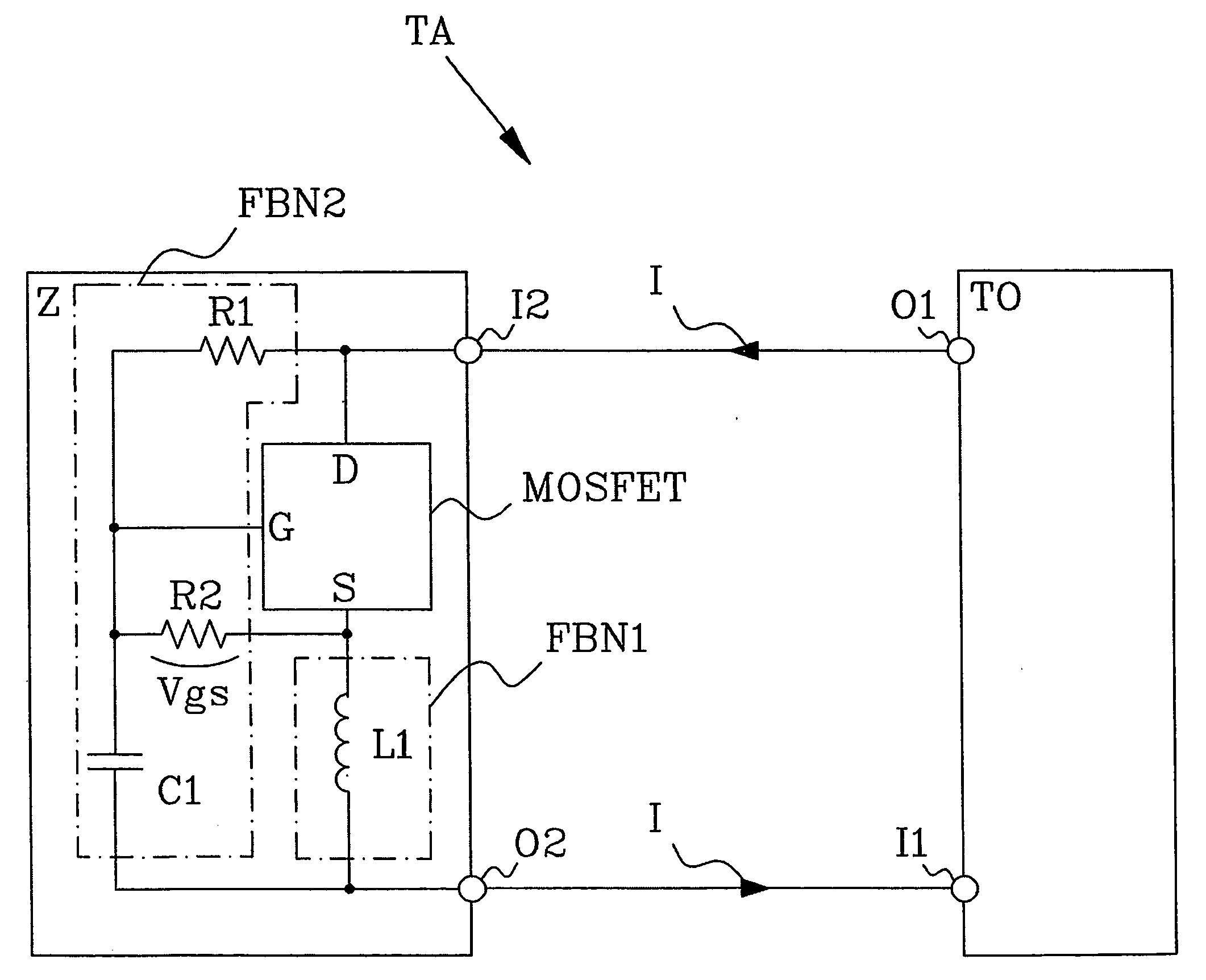
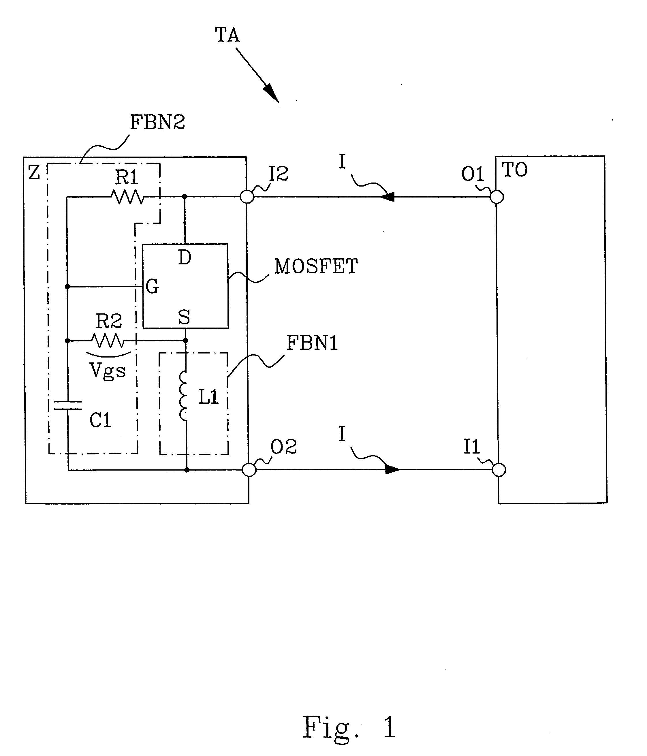
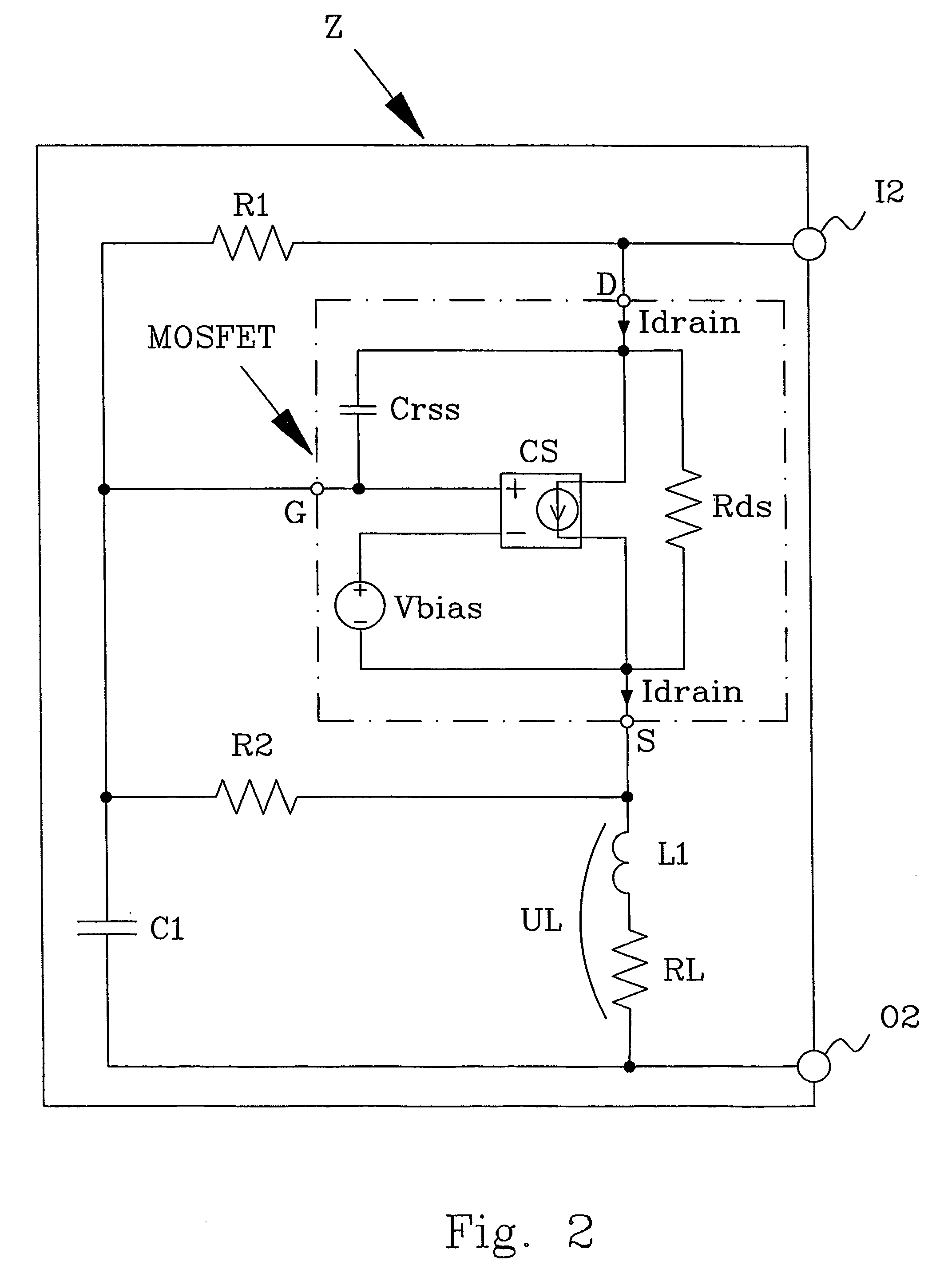
[0015] In FIG. 1 is disclosed a test arrangement TA comprising an active load arrangement Z connected to a test object TO. The active load arrangement provides proper output load to the object under test. The test object, which for example can be a POTS line interface circuit in a telecommunication system, comprises an object output O1 and an object input I1. The load arrangement Z comprises an arrangement input I2 associated with the object output O1. The arrangement Z also comprises an arrangement output O2 associated with the object input I1. The load arrangement Z further comprises a MOSFET with a drain D, a gate G and a source S. The semiconductor in this example is of the type IRF610. The drain D is connected to the arrangement input I2. A first resistance R1, in the example 2,2E6 ohm, is connected between the drain D and the gate G. A second resistance R2, in the example 2,2E6 ohm, is connected between the gate G and the source S. A capacitor C1, in the example 6,8 μF, is con...


PUM


Abstract

An active load arrangement is used to provide proper output load to an object TO under test. The arrangement Z comprises a voltage_controlled transistor MOSFET having a source S, a gate G and a drain D. The drain D is associated with the gate G and connected to an arrangement input I2 associated with an output O1 of the object under test. The source S is connected to an arrangement output O2 associated with an input I1 of the object under test. A feedback arrangement is connected to the source S and the gate G. The feedback arrangement changes phase and amplitude of the gate-to-source voltage by varying frequency in order to obtain low impedance at low frequencies and high impedance at high frequencies.

Description

TECHNICAL FIELD OF THE INVENTION [0001] The present invention relates to an active load arrangement providing proper output load to a device under test. DESCRIPTION OF RELATED ART [0002] Automatic test equipment is frequently employed to run diagnostic tests on integrated circuit devices. A purpose of a testing device is to ensure that integrated circuits under test provide the proper output voltages given the input stimulus of the tester. It is necessary that such devices simulate the proper output load. In the U.S. Pat. No. 4,712,058 is disclosed an active load network for a device under test and for turning on either a current source or a current sink to properly load its output. The current sink and current source each comprises a pair of CMOS transistors connected in series. An active load network that provides low resistance for direct current DC and high impedance for alternating current AC is often necessary when testing an object of for example line interface type. This typ...

Claims


Application Information

Patent Timeline
Patent Type & Authority Applications(United States)
IPC IPC(8): H03B1/00G01R31/316H03F1/56H03H11/46
CPCG01R31/316H03H11/46H03F2200/492H03F1/56
Inventor BLADH, MATS
Owner TELEFON AB LM ERICSSON (PUBL)
Why Eureka
Try Eureka