Method for manufacturing low-temperature poly-silicon thin film transistor

a thin film transistor and polysilicon technology, applied in the field of display panels, can solve the problems of complex manufacturing procedure, inability to meet the requirements of large size and high resolution display devices, and low carrier mobility of a-si materials, so as to reduce manufacturing costs, simplify manufacturing procedures, and eliminate the effect of source-drain contact layer

Inactive Publication Date: 2019-03-28
WUHAN CHINA STAR OPTOELECTRONICS TECH CO LTD
View PDF11 Cites 3 Cited by
  • Summary
  • Abstract
  • Description
  • Claims
  • Application Information

AI Technical Summary

Benefits of technology

[0031]In conclusion, in the method for manufacturing the low-temperature poly-silicon thin film transistor according to the present disclosure, an ohmic contact layer is deposited through PECVD method during the procedure of forming the source-drain contact layer, and meanwhile, the reaction gas used therein contains diborane. In this manner, the boron ions can enter into the source-drain contact layer during deposition of the ohmic contact layer, so that the impedance of the source-drain contact layer can be reduced, and the contact impedances thereof with the source and the drain become smaller. According to this method, a mask is not needed to define an implanted region of boron ions. Therefore, a process of implanting the boron ions can be saved; the manufacturing procedure can be simplified; and the manufacturing cost can be reduced. According to the present disclosure, since the LTPS-TFT is manufactured through the method disclosed herein, the manufacturing cost can be reduced.

Problems solved by technology

However, carrier mobility of a-Si material is quite low, which cannot meet the requirements of large size and high resolution display devices, especially the requirements of the next generation active matrix organic light emitting display devices.
The manufacturing procedure is complicated and the manufacturing cost is high.
Hence, how to simplify the manufacturing procedure of LTPS-TFT and reduce the manufacturing cost thereof becomes an urgent problem to be solved.

Method used


Image

  • Method for manufacturing low-temperature poly-silicon thin film transistor
  • Method for manufacturing low-temperature poly-silicon thin film transistor
  • Method for manufacturing low-temperature poly-silicon thin film transistor

Examples


embodiment 1

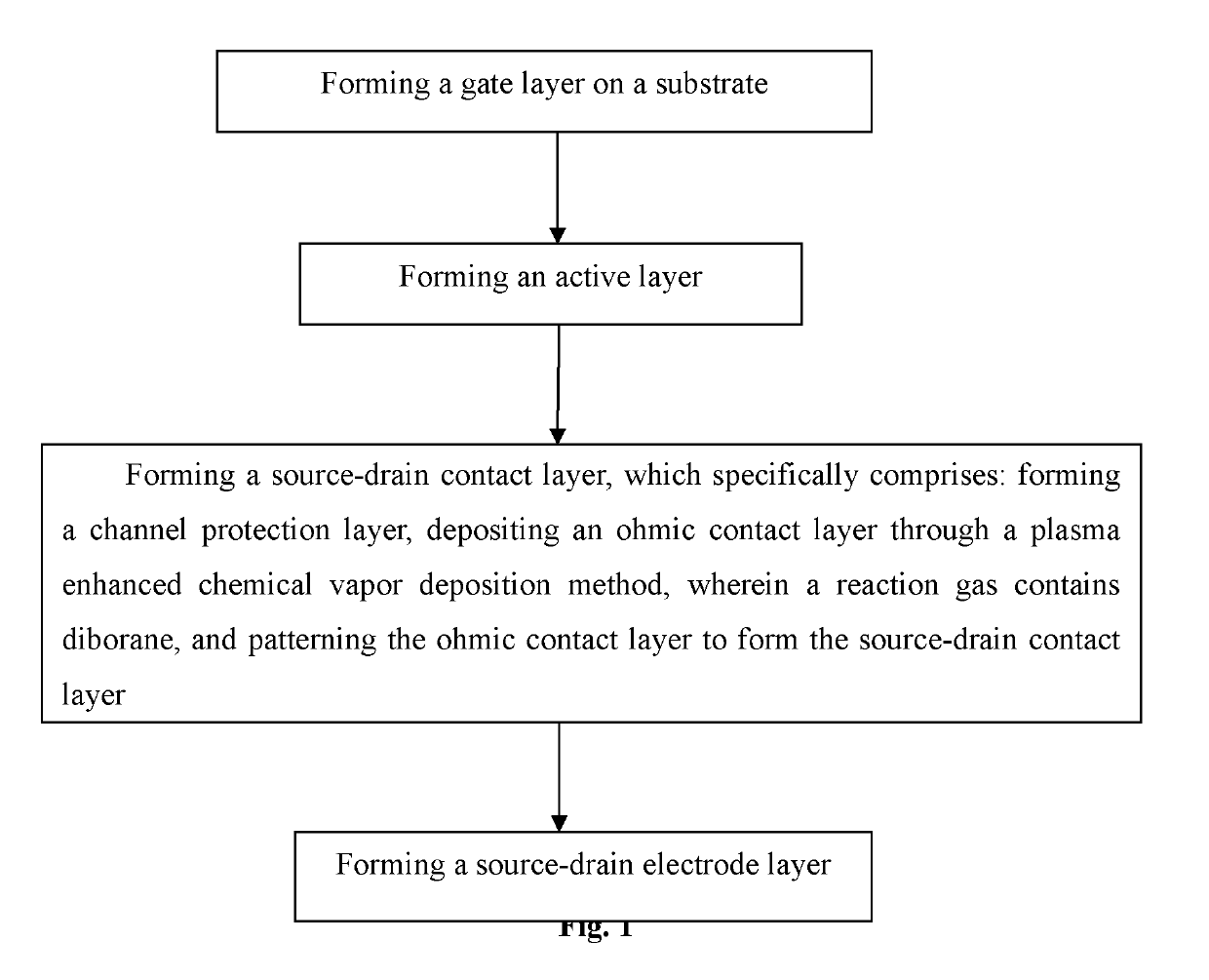
[0041]FIG. 1 shows a method for manufacturing a low-temperature poly-silicon thin film transistor according to the present embodiment. The method comprises steps of:

[0042]in step S11, a gate layer is formed on a substrate;

[0043]in step S12, an active layer is formed;

[0044]in step S13, a source-drain contact layer is formed; and

[0045]in step S14, a source-drain electrode layer is formed.

[0046]Each step will be described in detail below.

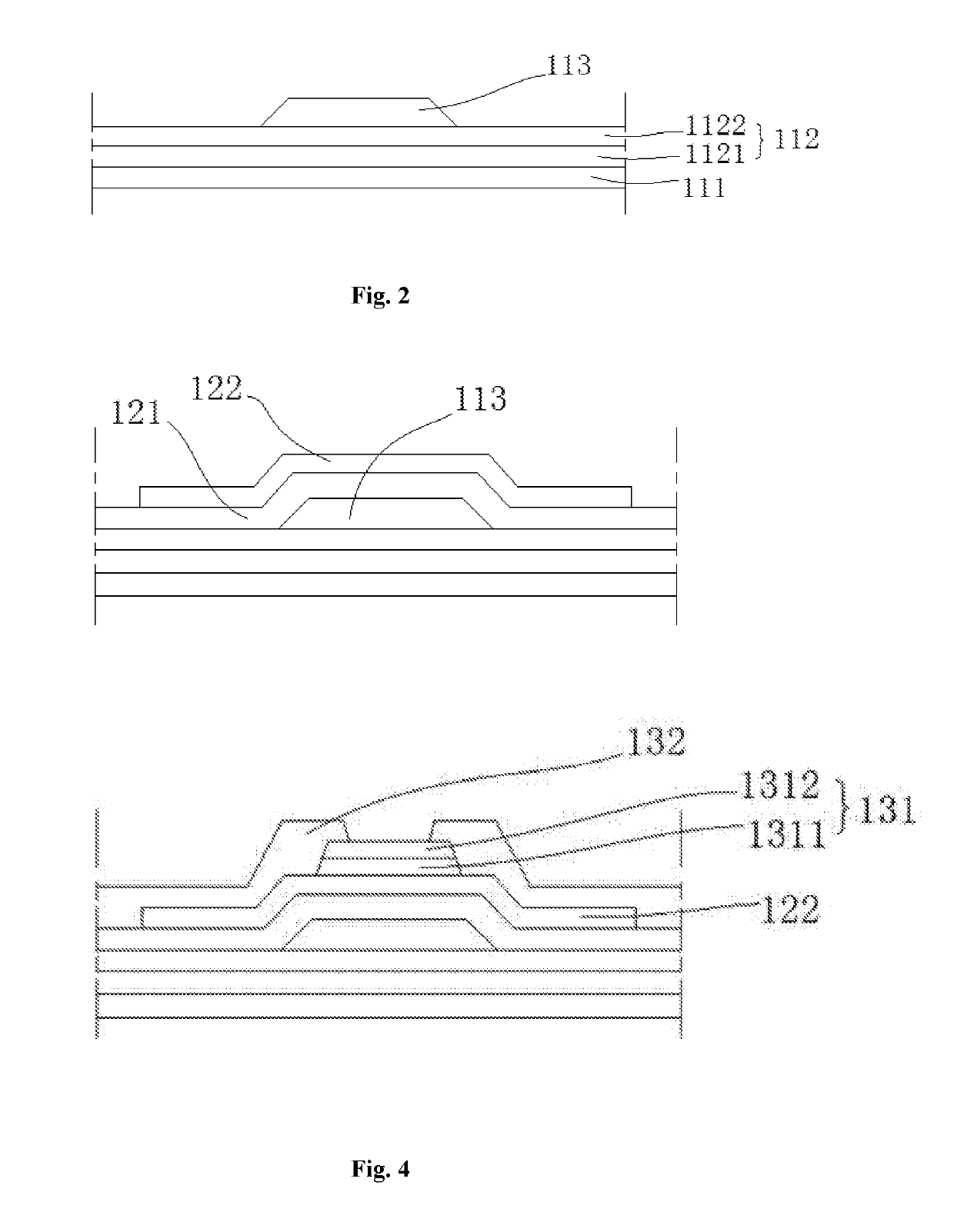
[0047]In step S11, the gate layer is formed on the substrate. As shown in FIG. 2, first, a buffer layer 112 is manufactured on an entire surface of a substrate 111, and the buffer layer 112 comprises a silicon nitride layer 1121 and a silicon oxide layer 1122. Of course, according to other embodiments, the buffer layer 112 can comprise only the silicon nitride layer 1121 or the silicon oxide layer 1122. Then, a first metal layer is deposited on the buffer layer 112. Preferably, a material that constitutes the first metal layer is molybdenum. According ...

embodiment 2

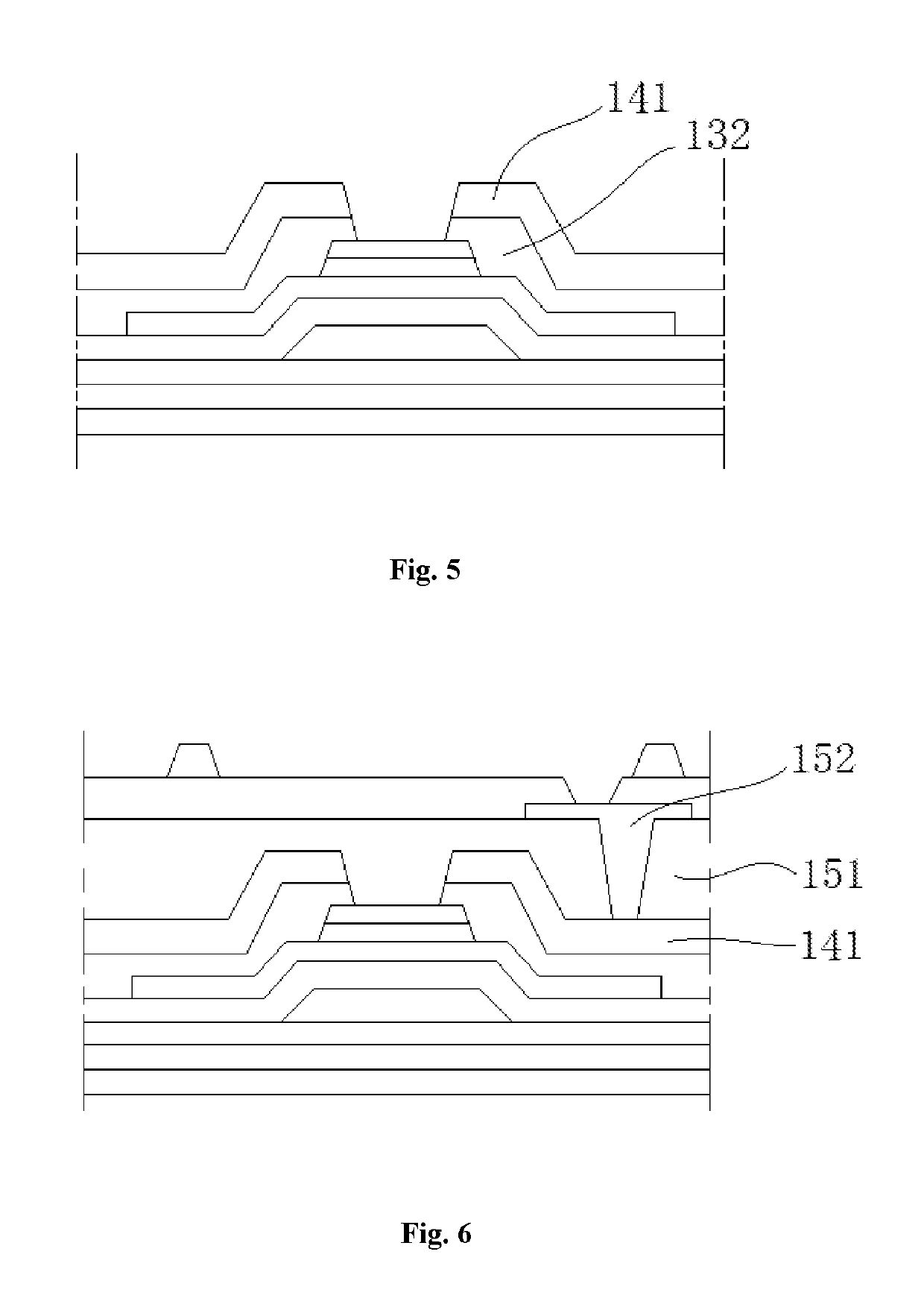
[0057]While manufacturing an array substrate containing the low-temperature poly-silicon thin film transistor manufactured by the aforesaid method, a step S15 is further comprised. As shown in FIG. 6, an organic photoresist planar insulating layer 151 is manufactured on the source-drain electrode layer 141, and then an Anode electrode layer 152 is manufactured. Then a pixel-defining layer (PDL) and a pillar spacer (PS) layer are manufactured.

[0058]Finally, it should be noted that, the above embodiments are only used to explain the technical solution of the present disclosure and shall not be construed as limitation.


PUM


Abstract

Disclosed is a method for manufacturing a low-temperature poly-silicon thin film transistor, which relates to the technical field of display panel. The method comprises steps of: forming a gate layer, an active layer, a source-drain contact layer and a source-drain electrode in sequence on a substrate. The step of forming the source-drain contact layer includes sub steps of: forming a channel protection layer; depositing an ohmic contact layer using a reaction gas containing diborane and through a plasma enhanced chemical vapor deposition method; and patterning the ohmic contact layer to form the source-drain contact layer. During deposition of the ohmic contact layer, boron ions can enter into the source-drain contact layer. According to this method, a mask is not needed to define an implanted region of boron ions. Therefore, a procedure of implanting the boron ions can be saved; the manufacturing procedure can be simplified; and the manufacturing cost can be reduced.

Description

CROSS-REFERENCE TO RELATED APPLICATIONS[0001]This application claims the priority of Chinese patent application CN 201710249455.0, entitled “Method for manufacturing low-temperature poly-silicon thin film transistor” and filed on Apr. 17, 2017, the entirety of which is incorporated herein by reference.FIELD OF THE INVENTION[0002]The present disclosure relates to the technical field of display panel, and in particular, to a method for manufacturing a low-temperature poly-silicon thin film transistor.BACKGROUND OF THE INVENTION[0003]In pixel units of various display devices, thin film transistors (TFT) for driving the display devices by applying driving voltages are widely used. An amorphous silicon (a-Si) material with good stability and workability is always used in an active layer of a TFT. However, carrier mobility of a-Si material is quite low, which cannot meet the requirements of large size and high resolution display devices, especially the requirements of the next generation ...

Claims


Application Information

Patent Timeline
Patent Type & Authority Applications(United States)
IPC IPC(8): H01L21/02H01L29/49H01L29/66H01L29/786
CPCH01L21/02595H01L21/02532H01L21/02675H01L21/02669H01L29/4908H01L29/66765H01L29/786H01L21/28556H01L29/78678
Inventor LI, SONGSHAN
Owner WUHAN CHINA STAR OPTOELECTRONICS TECH CO LTD
Why Eureka
Try Eureka