
Probe card for integrated circuits

Inactive Publication Date: 2007-03-29
STAR TECH INC
View PDF6 Cites 12 Cited by
  • Summary
  • Abstract
  • Description
  • Claims
  • Application Information

AI Technical Summary

Benefits of technology

[0009] The objective of the present invention is to provide a probe card for integrated circuits which uses ultrasonic energy to vibrate a probe pin of the probe card to scratch a dielectric layer on a pad of the integrated circuit so as to decrease the contact resistance between the probe pin and the pad, and method for cleaning the probe pin by the ultrasonic energy.
[0011] When the probe pin contacts a pad of an integrated circuit device under test, the ultrasonic generator can emit the ultrasonic energy to vibrate the probe pin so as to form a recess on a dielectric layer on the pad, and the probe pin is then pressed downward to contact the pad through the recess with low overdrive forming a signal path. Preferably, the ultrasonic energy can vibrate the probe pin in an XYZ 3-dimensional manner. In addition, the ultrasonic energy may vibrate the probe pin to brush the surface of the pad or scratch the dielectric layer on the surface of the pad when the probe pin contacts the surface of the pad of the integrated circuit device, with the ultrasonic energy preferably vibrating the probe pin in an XY 2-dimensional manner. Consequently, the contact resistance between the probe pin and the pad can be decreased due to improved contact between the probe pin and the pad with the dielectric removed.
[0013] Conventional technique must overdrive the probe pin continuously to scratch the dielectric layer on the surface of the pad, which is likely to result in a sliding probe pin or in collapse of the porous low-k dielectric material below the pad under high probe pressure, causing the dielectric structure between conductors to be damaged. Conversely, when the probe pin contacts the surface of the pad, the embodiment of the present invention uses ultrasonic energy to vibrate the probe pin to form the recess and then with low overdrive causing the probe pin to contract the pad, forming the signal path. Since the recess can automatically locate the position of the probe pin to avoid the occurrence of the sliding probe, the pad can be contacted precisely.
[0014] In addition, the probe pin can scratch the dielectric layer without overdriving the probe pin since the ultrasonic energy vibrates the probe pin to form the recess before the probe pin is pressed downward to scratch the dielectric layer at the precise location of the recess. Consequently, the present invention can prevent the porous low-k dielectric material below the pad from collapsing to maintain the dielectric structure between conductors since the probe pin can scratch the dielectric layer on the pad without overdriving.
[0015] Further, ultrasonic energy may be used to vibrate the probe pin to brush the surface of the pad to clear the dielectric layer on the pad. The probe pin then contacts the pad of the integrated circuit device, and the contact resistance can be decreased as a result of improved contact between the probe pin and the pad. In addition, ultrasonic energy can also be used to vibrate the probe pin to remove contaminants during tests.

Problems solved by technology

As the semiconductor fabrication technique proceeds into the nanometer scale, the line width and the pitch shrink correspondingly, which results in RC-delay effect due to an increased conductor resistance and capacitance between conductors.
RC-delay has many negative influences such as a decreased signal propagation speed, an increased cross talk noise and power consumption, wherein the decreased signal propagation speed is the most serious one.
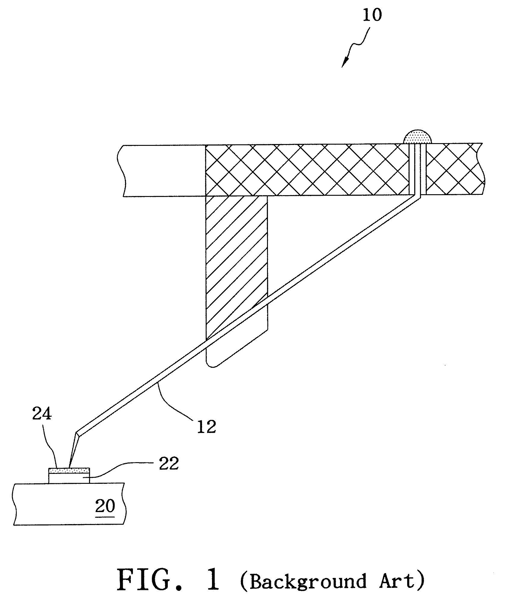
But, the porous low-k dielectric material used in the advanced integrated circuit fabrication process possesses lower mechanical properties, which can not sustain the applied force as the probe pin 12 is overdriven above 70 micrometers.
This destroys the dielectric structure between conductors and the integrated circuit device 20 fails or is damaged.
However, the cleaning process is controlled by the test machine and requires a length of time, reducing efficiency.
Further, the conventional cleaning process can not completely remove all contaminants, and some contaminants may remain on the probe pin 12.
More particularly, the brushing movement of the cleaning process often damages the probe pin 12.

Method used


Image

  • Probe card for integrated circuits
  • Probe card for integrated circuits
  • Probe card for integrated circuits

Examples


first embodiment

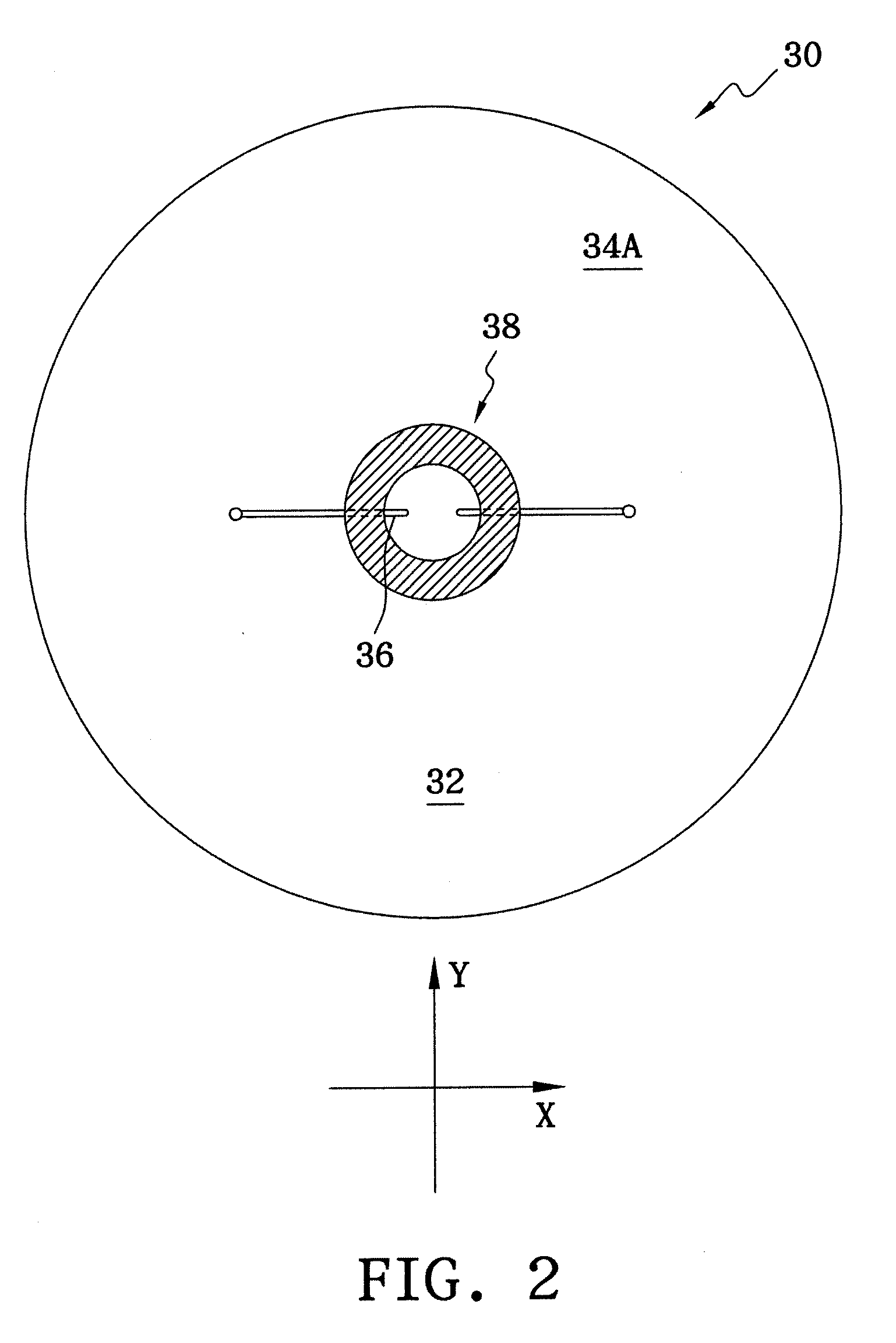
[0021]FIG. 2 and FIG. 3 illustrate a probe card 30 according to the present invention. The probe card 30 comprises a first substrate 32, a plurality of probe pins 36 positioned on a first surface 34A of the first substrate 32, and an ultrasonic generator 40 positioned on a second surface 34B of the first substrate 32. The ultrasonic generator 40 may be made of piezoelectric material such as lead zirconate titanate (PZT) to generate ultrasonic energy to vibrate the probe pin 36, and acquire operation power from an external power supply 50. Alternatively, the ultrasonic generator 40 can acquire operation power from the probe card 30 as well. Further, the ultrasonic generator 40 and the power supply 50 may be incorporated in a test head of a test machine (not shown in the drawing), and the ultrasonic generator 40 can acquire operation power from a power supply of the test head to generate ultrasonic energy to vibrate the probe pin 36 when the probe card 30 is assembled to the test head...

second embodiment

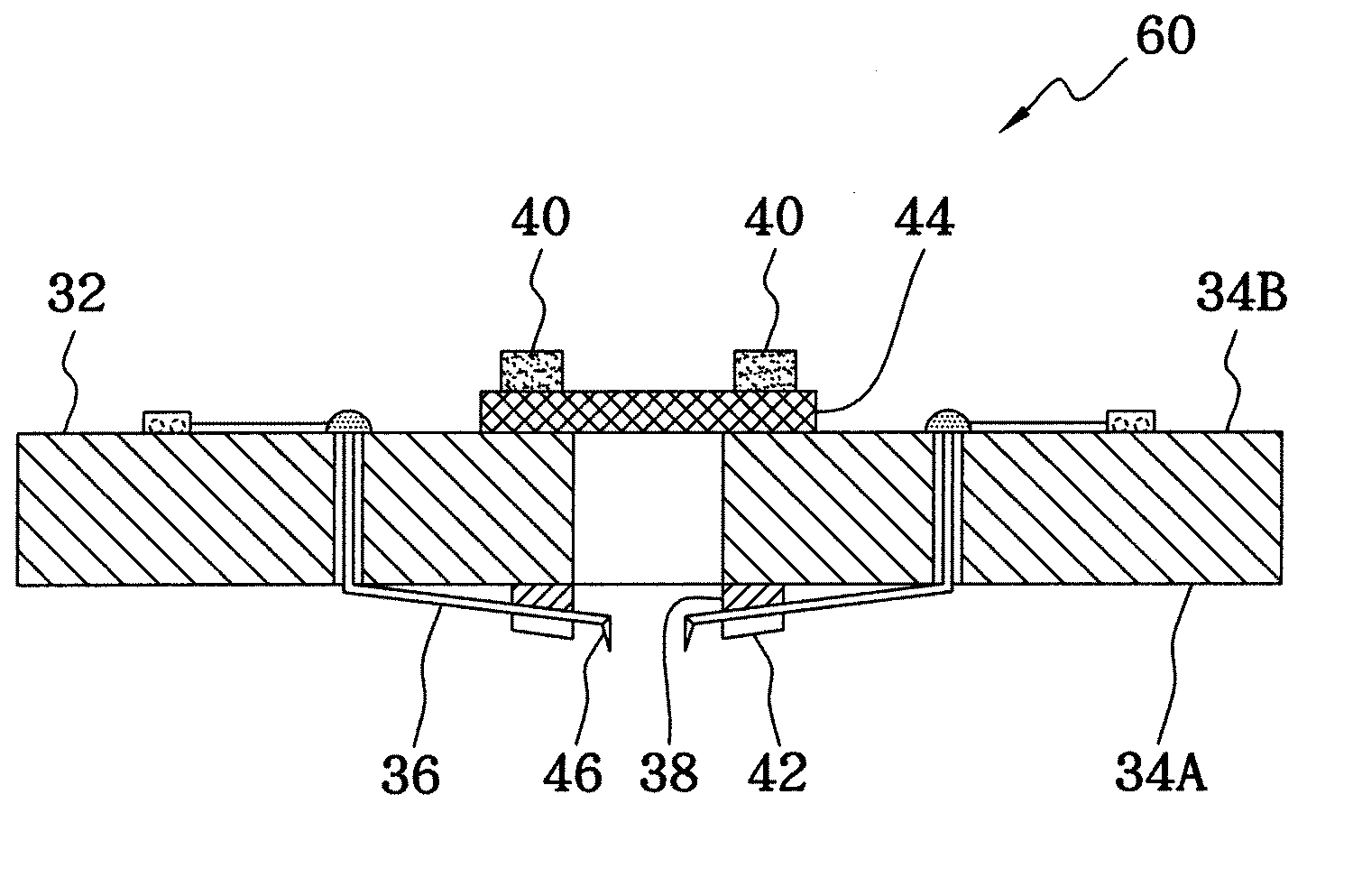
[0026]FIG. 6 illustrates a probe card 60 according to the present invention. Compared to the probe card 30 shown in FIG. 4, the ultrasonic generator 40 of the probe card 60 shown in FIG. 6 is positioned on a second substrate 44, which can be assembled to the second surface 34B of the first substrate 32. Particularly, the ultrasonic generator 40 can be positioned anywhere or on an external substrate such as the second substrate 44, and coupled to the first substrate 42 to generate the ultrasonic energy to vibrate the probe pin 36 when the probe card 60 is used to perform electrical testing. Further, the ultrasonic generator 40 can connect to the first substrate 32 or the probe pin 36 in any manner so long as the generated ultrasonic energy can drive the probe pin 36 to vibrate in a reciprocating pattern to scratch the dielectric layer 24.

[0027] As an alternative to the conventional technique for cleaning the probe pin, the present invention can be used to clean the probe pin 36 by pl...


PUM


Abstract

A probe card for integrated circuit devices comprises a printed circuit board, at least one probe pin positioned on the printed circuit board, and at least one ultrasonic generator configured to generate ultrasonic energy. When the probe pin contacts a pad, the ultrasonic generator emits ultrasonic energy to vibrate the probe pin so as to form a recess on the surface of a dielectric layer such as an oxide layer on the pad, and the probe pin is then pressed downward to scratch the dielectric layer to form a signal channel. While some contaminants such as oxide fragments usually adhere to the probe pin when the probe card is used to perform an electrical test of the integrated circuit device, the present invention can use ultrasonic energy to vibrate the probe pin so as to remove contaminants from the probe pin.

Description

BACKGROUND OF THE INVENTION [0001] 1. Field of the Invention [0002] The present invention relates to a probe card for integrated circuits, and more particularly, to a probe card for integrated circuits which uses ultrasonic energy to vibrate a probe pin of the probe card to scratch a dielectric layer on a pad of the integrated circuit so as to decrease the contact resistance between the probe pin and the pad. [0003] 2. Description of the Related Art [0004] Generally, it is necessary to test electrical properties of integrated circuit devices on the wafer level to verify that the integrated circuit device satisfies the product specification. Integrated circuit devices with all electrical properties satisfying specifications are selected to continue through the subsequent packaging process, while other devices are discarded to avoid additional packaging cost. Another electrical property test is performed on the integrated circuit device after the packaging process is completed to siev...

Claims


Application Information

Patent Timeline
IPC IPC(8): G01R31/02
CPCG01R1/06711G01R1/06772G01R1/06727G01R31/2891G01R1/07342
Inventor LOU, CHOON-LEONGHSU, MEI-SHU
Owner STAR TECH INC
Learn More