Semiconductor device and semiconductor device manufacturing method

a semiconductor device and manufacturing method technology, applied in the direction of semiconductor devices, basic electric elements, electrical appliances, etc., can solve the problems of affecting the low-voltage operation of transistors, deteriorating drain current rising characteristics in subthreshold regions, and inferior crystallinity of silicon thin films of upper and lower layers. to achieve good crystalline quality

Inactive Publication Date: 2007-04-05
SEIKO EPSON CORP +1
View PDF3 Cites 204 Cited by
  • Summary
  • Abstract
  • Description
  • Claims
  • Application Information

AI Technical Summary

Benefits of technology

[0012] This configuration makes it possible to increase flexibility in the arrangement of a back gate electrode and arrange a back gate electrode in a part where concentration of an electric field occurs, without being limited by the arrangement of a gate electrode, source and drain contacts, and the like. Accordingly, it becomes possible to increase flexibility in the design of a field-effect transistor, and an increase in the withstand voltage of a field-effect transistor can be ensured.
[0030] This configuration makes it possible to make etching rates of the first and third single-crystal semiconductor layers higher than etching rates of the single-crystal semiconductor substrate and the second and fourth single-crystal semiconductor layers while lattice matching the single-crystal semiconductor substrate and the first to fourth single-crystal semiconductor layers to each other. Accordingly, it becomes possible to form the second and fourth single-crystal semiconductor layers with good crystalline quality on the first and third single-crystal semiconductor layers, respectively, and ensure insulation between the second and fourth single-crystal semiconductor layers and the single-crystal semiconductor substrate without impairing the qualities of the second and fourth single-crystal semiconductor layers.

Problems solved by technology

As a result, the crystallinity of the silicon thin film of the upper layer is inferior to that of the silicon thin film of the lower layer.
Additionally, in a conventional semiconductor integrated circuit, as the channel length of a transistor decreases along with its miniaturization, the rising characteristics of a drain current in a subthreshold region deteriorate.
This interferes with low-voltage operation of the transistor and increases an off-leak current.
Such an off-leak current not only increases the power consumed during operation or standby but also may constitute a major factor in a breakdown of the transistor.

Method used


Image

  • Semiconductor device and semiconductor device manufacturing method
  • Semiconductor device and semiconductor device manufacturing method
  • Semiconductor device and semiconductor device manufacturing method

Examples


first embodiment

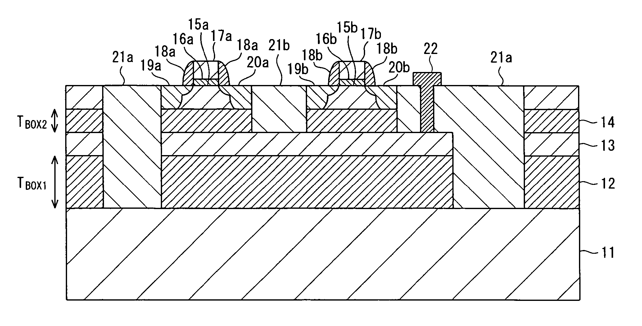
[0045]FIG. 1 is a section view showing a schematic configuration of a semiconductor device according to the present invention.

[0046] In FIG. 1, a buried oxide film 12 is formed on a single-crystal semiconductor substrate 11, and a single-crystal semiconductor layer 13 constituting aback gate electrode is formed on the buried oxide film 12. Further, a buried oxide film 14 is formed on the single-crystal semiconductor layer 13, and mesa-isolated single-crystal semiconductor layers 15a and 15b are stacked on the buried oxide film 14. Note that Si can be used as a material for the single-crystal semiconductor substrate 11, single-crystal semiconductor layers 13, 15a and 15b. A film thickness TBOX1 of the buried oxide film 12 is preferably larger than a film thickness TBOX2 of the buried oxide film 14. The single-crystal semiconductor layer 13 is subjected to element isolation by buried insulators 21a, and the single-crystal semiconductor layers 15a and 15b are subjected to element isola...

second embodiment

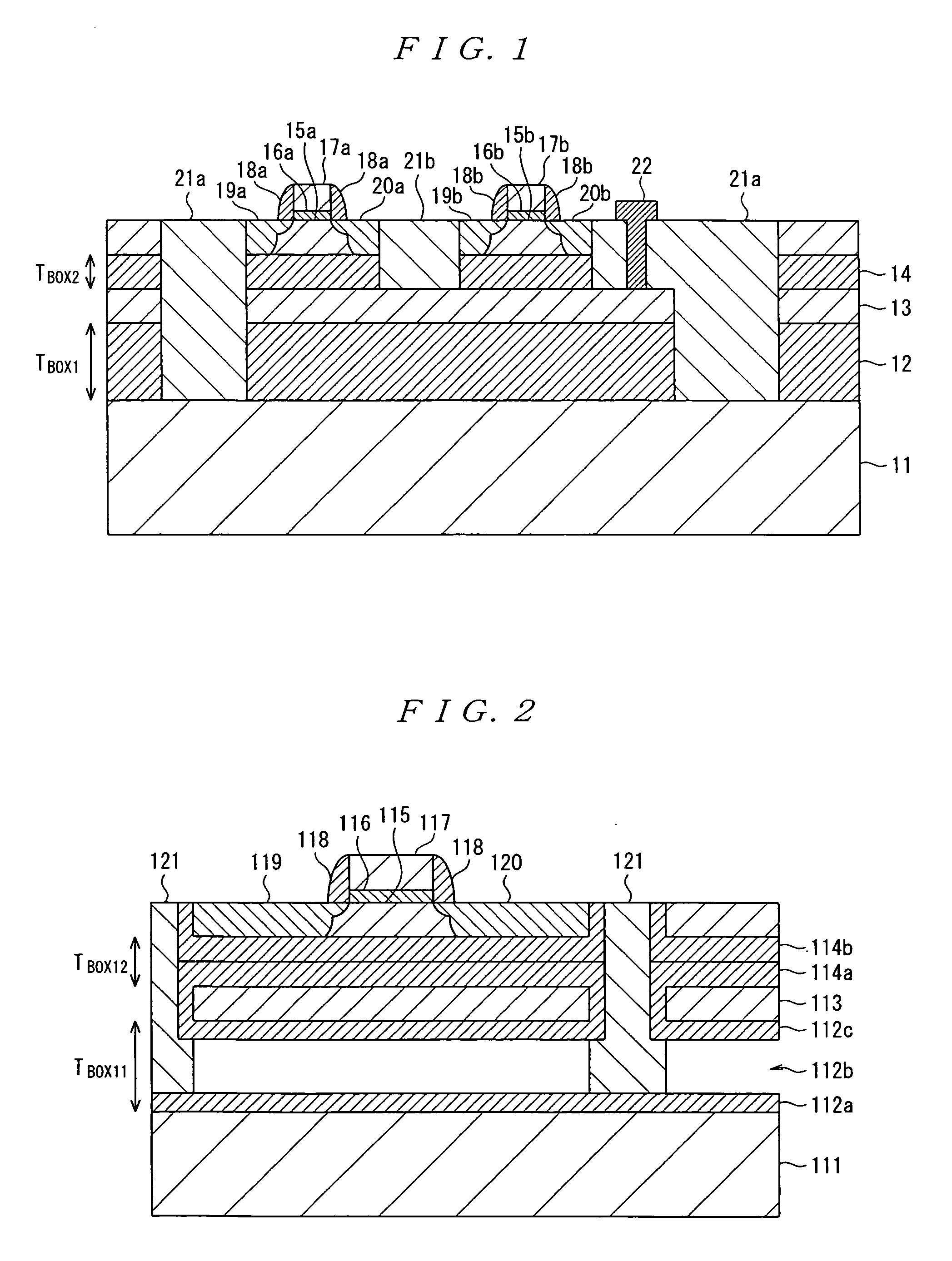
[0052]FIG. 2 is a section view showing a schematic configuration of a semiconductor device according to the present invention.

[0053] In FIG. 2, a single-crystal semiconductor layer 113 constituting a back gate electrode via a cavity portion 112b whose upper and lower surfaces are covered with surface oxide films 112a and 112c is formed on a single-crystal semiconductor substrate 111. Further, buried oxide films 114a and 114b are successively formed on the single-crystal semiconductor layer 113, and a single-crystal semiconductor layer 115 is laminated on the buried oxide film 114b. Note that Si can be used as a material of the single-crystal semiconductor substrate 111 and the single-crystal semiconductor layers 113 and 115. The total film thickness TBOX11 of the surface oxide films 112a and 112c and the cavity portion 112b is preferably larger than the total film thickness TBOX12 of the buried oxide films 114a and 114b. The single-crystal semiconductor layers 113 and 115 are subjec...

third embodiment

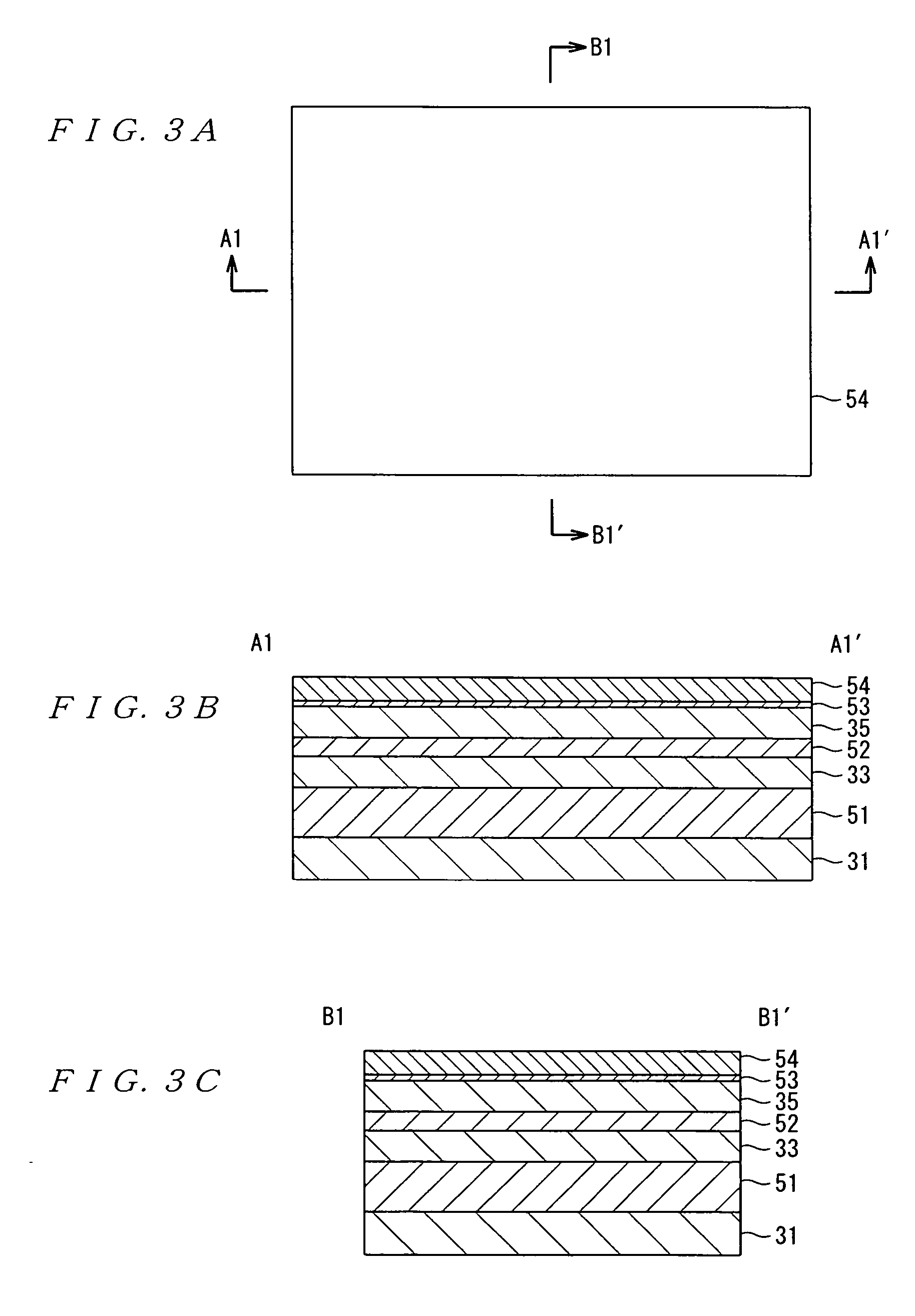
[0056]FIGS. 3A to 13A are plan views showing a semiconductor device manufacturing method according to the present invention; FIGS. 3B to 13B, section views taken along the lines A1-A1′ to A11-A11′ in FIGS. 3A to 13A, respectively; and FIGS. 3C to 13C, section views taken along the lines B1-B11′ to B11-B11′ in FIGS. 3A to 13A, respectively.

[0057] In FIGS. 3A to 3C, single-crystal semiconductor layers 51, 33, 52, and 35 are sequentially stacked on a single-crystal semiconductor substrate 31 by epitaxial growth. At this time, a film thickness of the single-crystal semiconductor layer 51 can be made larger than a film thickness of the single-crystal semiconductor layer 52. As materials for the single-crystal semiconductor layers 51 and 52, ones whose etching rates are higher than those of the single-crystal semiconductor substrate 31 and single-crystal semiconductor layers 33 and 35 can be used. In particular, if the single-crystal semiconductor substrate 31 is made of Si, it is prefera...


PUM


Abstract

A semiconductor device includes a back gate electrode composed of a first single-crystal semiconductor layer formed on a first insulating layer; a second insulating layer formed on the first single-crystal semiconductor layer and having a film thickness smaller than a film thickness of the first insulating layer; a second single-crystal semiconductor layer formed on the second insulating layer; a gate electrode formed on the second single-crystal semiconductor layer; and source and drain layers that are formed on the second single-crystal semiconductor layer and arranged on respective sides of the gate electrode.

Description

[0001] The entire disclosure of Japanese Patent Application No. 2005-288877, filed Sep. 30, 2005 is expressly incorporated by reference herein. BACKGROUND OF THE INVENTION [0002] 1. Field of the Invention [0003] The present invention relates to a semiconductor device and a semiconductor device manufacturing method and, more particularly, to ones suitable for application to an SOI (Silicon On Insulator) transistor provided with a back gate electrode. [0004] 2. Description of the Related Art [0005] A field-effect transistor formed on an SOI (Silicon On Insulator) substrate is attracting attention for its usefulness in terms of ease of element isolation, freedom from latch-up, small source / drain junction capacitances, and the like. [0006] For example, JP-A-10-261799 discloses a method of irradiating an amorphous or polysilicon layer formed on an insulating film with ultraviolet light beams in a pulsed manner to form, on the insulating film, a polysilicon film having almost-cubic single...

Claims


Application Information

Patent Timeline
Patent Type & Authority Applications(United States)
IPC IPC(8): H01L29/04
CPCH01L21/84H01L27/1203
Inventor KATO, JURIOKA, HIDEAKIKANEMOTO, KEIHARA, TOSHIKISAKAI, TETSUSHI
Owner SEIKO EPSON CORP
Why Eureka
Try Eureka