Method of plasma etching of high-k dielectric materials

a dielectric material and plasma etching technology, applied in the direction of decorative surface effects, electrical appliances, decorative arts, etc., can solve the problems of affecting the performance of the transistor, the inability to etch using conventional oxide etchants to form into the gate structure without damaging other parts, and the limited use of hafnium oxide in the semiconductor devi

Inactive Publication Date: 2007-04-05
APPLIED MATERIALS INC
View PDF35 Cites 16 Cited by
  • Summary
  • Abstract
  • Description
  • Claims
  • Application Information

AI Technical Summary

Problems solved by technology

With such a thin dielectric, electrons can propagate from the polysilicon gate electrode into the transistor channel causing the transistor to operate improperly or become defective.
However, hafnium-oxide is such a stable dielectric material that it is very difficult to etch using conventional oxide etchants to form into gate structures without damaging other layers of material residing on the wafer.
As such, hafnium-oxide has found limited use in semiconductor devices.

Method used


Image

  • Method of plasma etching of high-k dielectric materials
  • Method of plasma etching of high-k dielectric materials
  • Method of plasma etching of high-k dielectric materials

Examples


Embodiment Construction

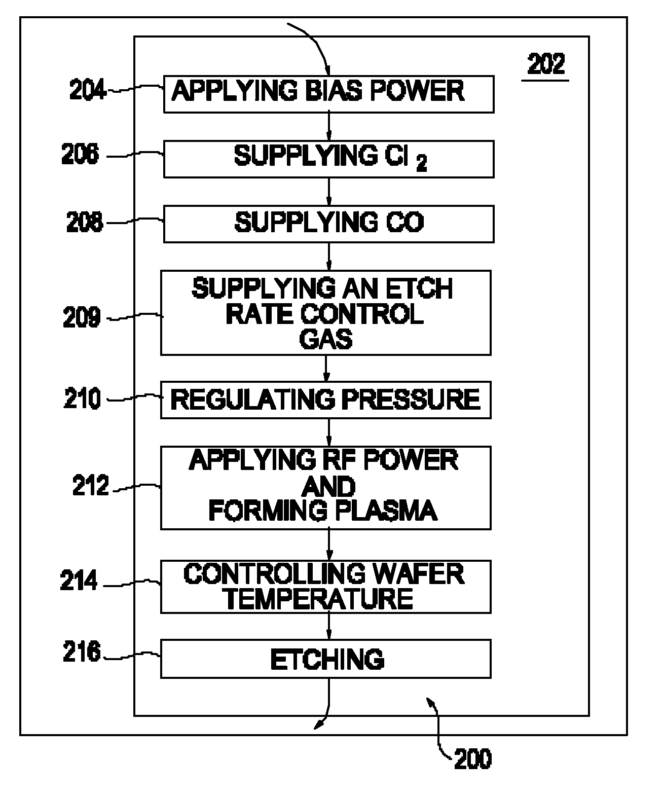
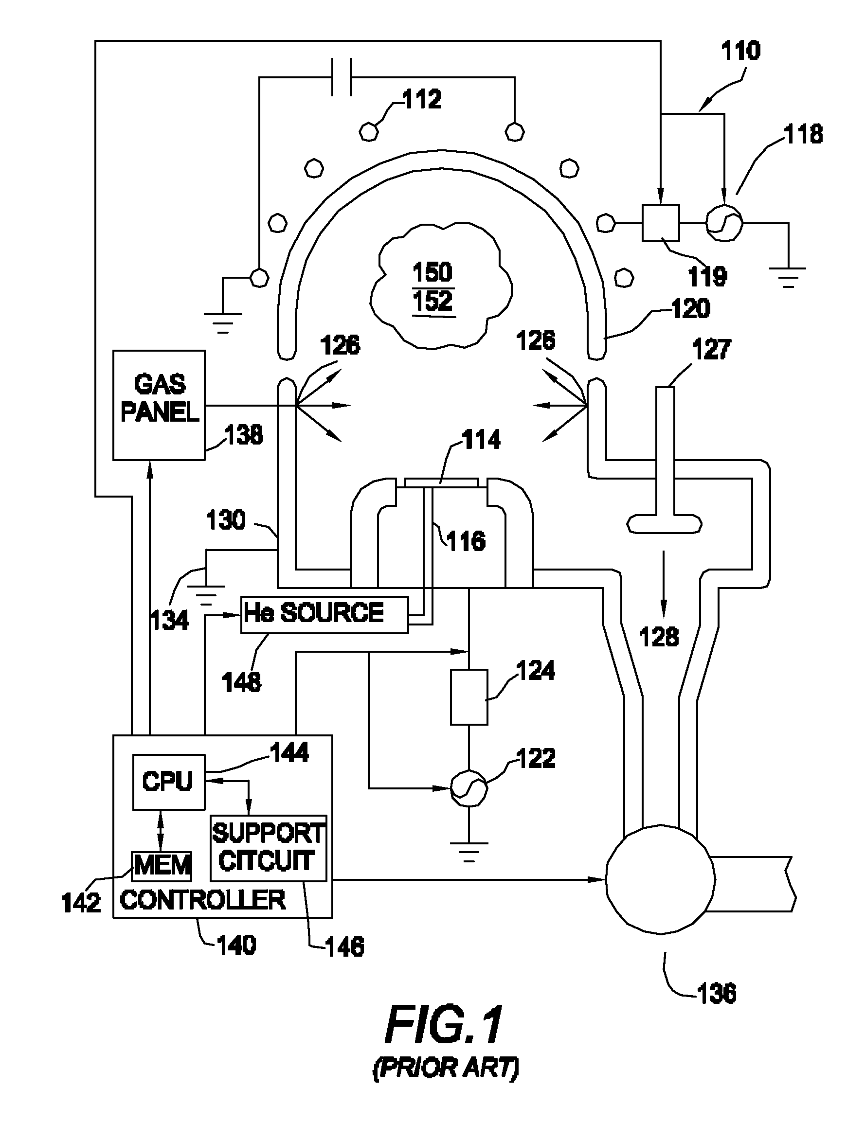
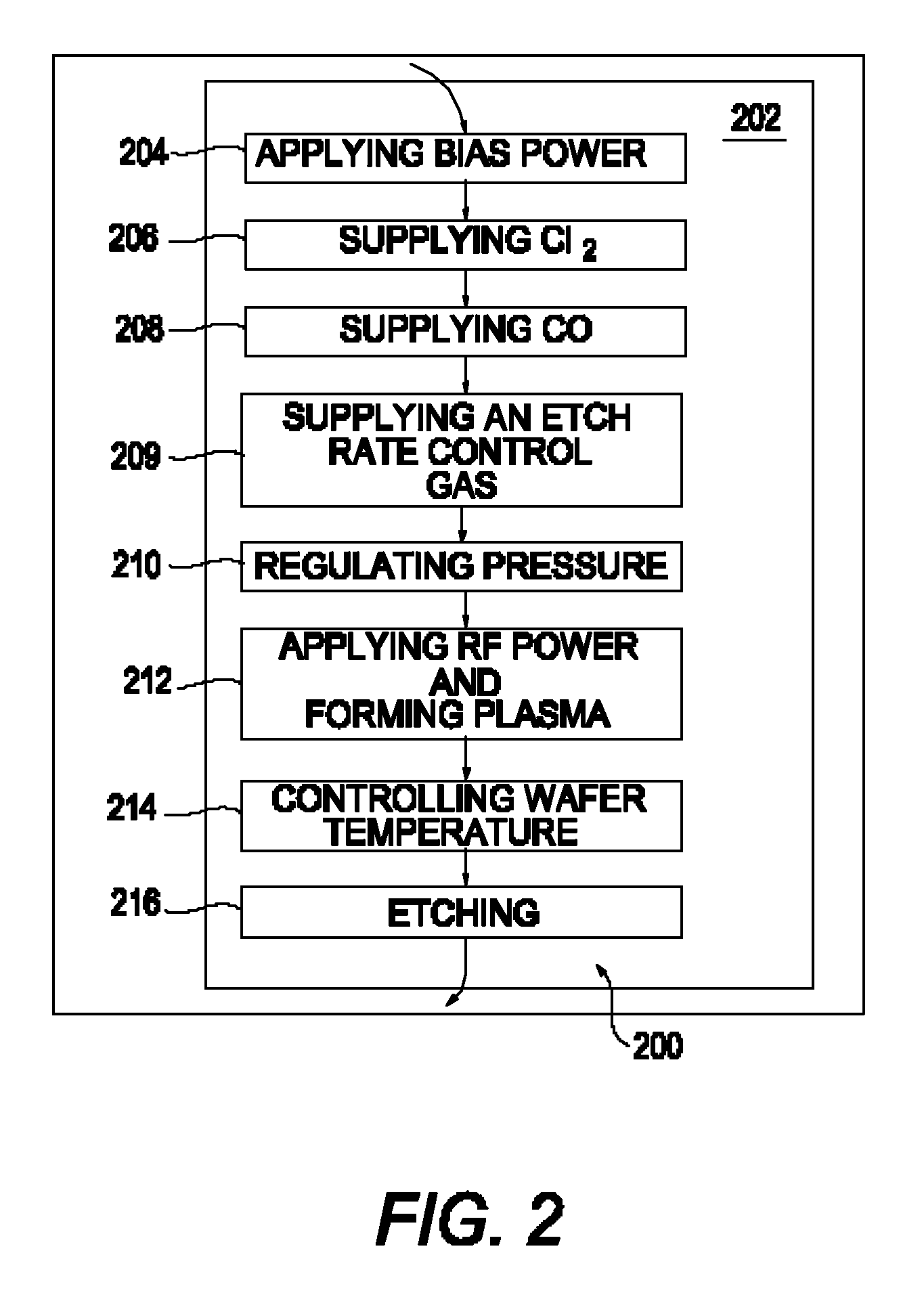
[0017] The present invention is a method of etching materials with high dielectric constants (high K materials have dielectric constants greater than 4.0) using a plasma generated from a gas (or gas mixture) comprising gases containing a halogen gas (such as Cl2, HCl and the like), a reducing gas (such as carbon monoxide (CO), and an etch rate control gas (at least one of Ar or O2) The high K materials include metal oxides such as HfO2, ZrO2, Al2O3, BST, PZT, ZrSiO2, HfSiO2, TaO2, and the like. The type of halogen gas is selected to best remove the metal from the dielectric layer and the type of reducing gas is selected to best remove the oxygen from the dielectric layer. The argon is a dilutant and the oxygen reacts with the carbon to form a carbonate. The argon dilutant aids in controlling the etch process by slowing the etch rate below 100 Å / min. Without an etch rate control gas, the etch rate can be more than 200 Å / min. Such etch rate control is especially important when etching...


PUM

PropertyMeasurementUnit
poweraaaaaaaaaa
temperatureaaaaaaaaaa
thicknessaaaaaaaaaa

Abstract

A method of etching high dielectric constant materials using a halogen gas, a reducing gas and an etch rate control gas chemistry.

Description

CROSS-REFERENCE TO RELATED APPLICATIONS [0001] This application is a continuation of co-pending U.S. patent application Ser. No. 10 / 143,397, filed May 9, 2002. The aforementioned related patent applications is herein incorporated by referenceBACKGROUND OF THE INVENTION [0002] 1. Field of Invention [0003] The present invention relates generally to a method of dry etching semiconductor wafers. More specifically, the invention relates to a method of etching high K dielectric materials using a gas mixture comprising a halogen gas and a reducing gas as well as an etch rate control gas. [0004] 2. Description of the Background Art [0005] Field effect transistors that are used in forming integrated circuit generally utilize a polysilicon gate electrodes deposited upon a gate dielectric that separates the electrode from the channel between source and drain regions. In prior art transistor structures, the gate dielectric is typically fabricated of silicon dioxide (SiO2). However, as integrate...

Claims


Application Information

Patent Timeline
Patent Type & Authority Applications(United States)
IPC IPC(8): C23F1/00H01L21/302C03C15/00H01L21/311H01L21/461
CPCH01L21/31122
Inventor JIN, GUANGXIANGNALLAN, PADMAPANIKUMAR
Owner APPLIED MATERIALS INC
Why Eureka
Try Eureka