Treatment of low dielectric constant films using a batch processing system

a processing system and dielectric constant technology, applied in the direction of coatings, metallic material coating processes, chemical vapor deposition coatings, etc., can solve the problems of poor adhesion of the barrier layer to the dielectric film, interconnect delay is a major limitation factor, and the film is less robust than the dielectric layer more traditional,

Active Publication Date: 2007-04-05
TOKYO ELECTRON LTD
View PDF28 Cites 74 Cited by
  • Summary
  • Abstract
  • Description
  • Claims
  • Application Information

AI Technical Summary

Benefits of technology

[0009] One aspect of the present invention is to reduce or eliminate any of the above-desc

Problems solved by technology

As is known to those in the semiconductor art, interconnect delay is a major limiting factor in the drive to improve the speed and performance of integrated circuits (IC).
While low-k materials are promising for fabrication of semiconductor circuits, the present inventors have recognized that these films also provide many challenges.
First, low-k films tend to be less robust than more traditional dielectric layers and can be damaged during wafer processing, such as by etch and plasma ashing processes generally used in patterning the dielectric layer.
Further, some low-k films tend to be highly reactive when damaged, particularly after patterning, t

Method used


Image

  • Treatment of low dielectric constant films using a batch processing system
  • Treatment of low dielectric constant films using a batch processing system
  • Treatment of low dielectric constant films using a batch processing system

Examples


Embodiment Construction

[0027] In the following description, in order to facilitate a thorough understanding of the invention and for purposes of explanation and not limitation, specific details are set forth, such as a particular geometry of the processing system and descriptions of various components. However, it should be understood that the invention may be practiced in other embodiments that depart from these specific details.

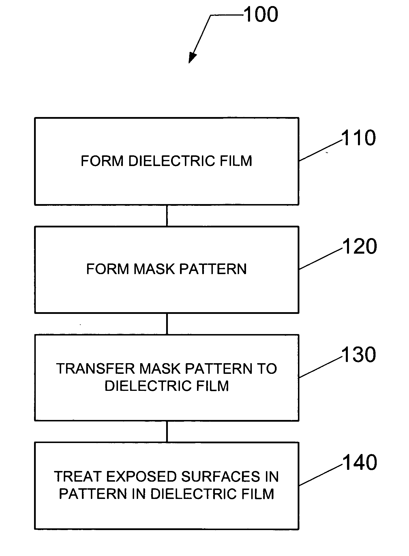
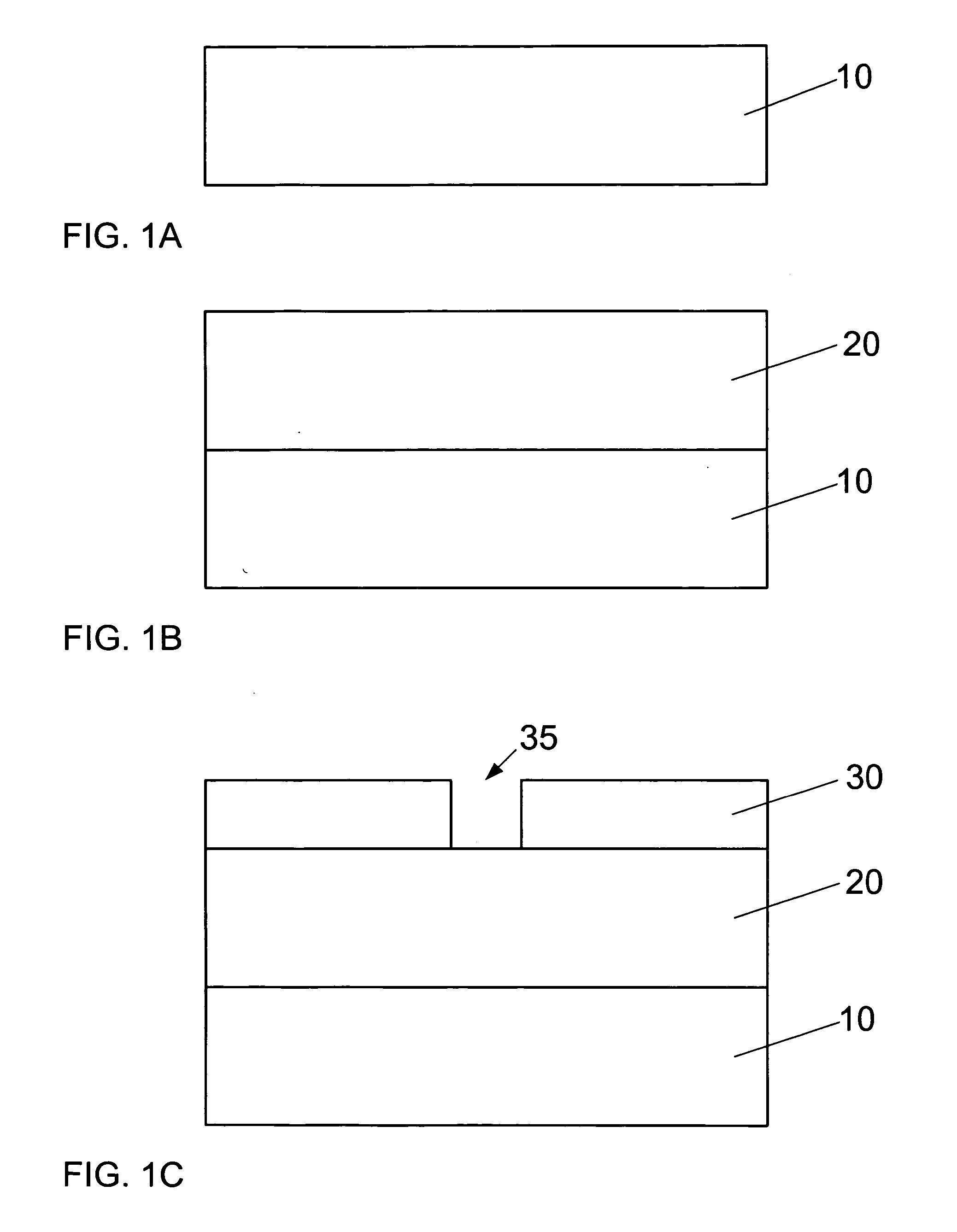
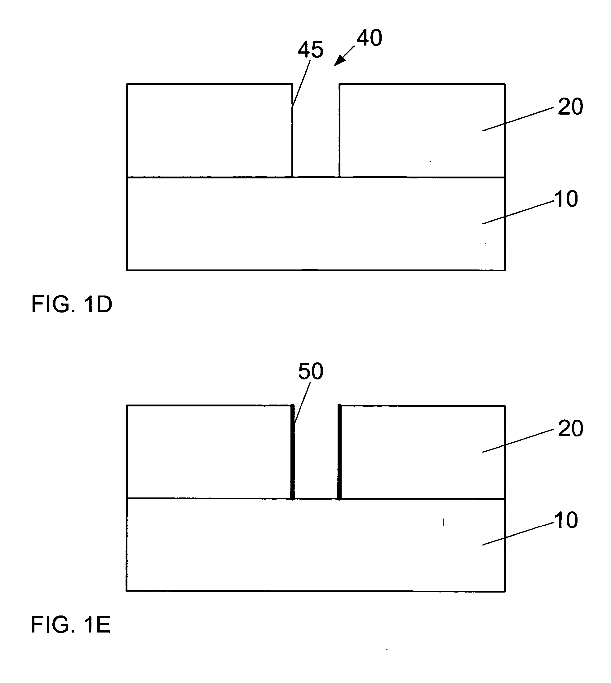
[0028] Referring now to the drawings, wherein like reference numerals designate identical or corresponding parts throughout the several views, FIGS. 1A through 1E present a schematic representation of a method of forming a pattern in a dielectric film and treating the exposed surfaces of the etched pattern in the dielectric film in order to perform at least one of drying, healing, sealing, or cleaning these surfaces. Additionally, FIG. 2 presents a flow chart 100 of performing the method according to an embodiment of the present invention. As shown in FIGS. 1A, 1B, and 2, a diel...


PUM

PropertyMeasurementUnit
Temperatureaaaaaaaaaa
Dielectric polarization enthalpyaaaaaaaaaa
Flow rateaaaaaaaaaa

Abstract

A method and system for treating a dielectric film in a batch processing system includes exposing at least one surface of the dielectric film to a treating compound including a CxHy containing compound, where x and y represent integers greater than or equal to unity. The plurality of wafers are heated when the treating compound is introduced. The dielectric film can include a low dielectric constant film with or without pores having an etch feature formed therein following dry etch processing.

Description

CROSS-REFERENCE TO RELATED APPLICATIONS [0001] This application is related to U.S. patent application Ser. No. 10 / 682,196, entitled “Method and system for treating a dielectric film”, Attorney docket no. 243414US, filed on Oct. 10, 2003; U.S. patent application Ser. No. 11 / 060,352, entitled “Method and system for treating a dielectric film”, Attorney docket no. 266479US, filed on Feb. 18, 2005; U.S. patent application Ser. No. 11 / ______, entitled “Plural treatment step process for treating low dielectric constant films”, Attorney docket no. 277839US, filed on even date herewith; and U.S. patent application Ser. No. 11 / ______, entitled “Plasma-assisted vapor phase treatment of low dielectric constant films using a batch processing system”, Attorney docket no. 277840 US, filed on even date herewith; the contents of which are incorporated by reference in their entirety.BACKGROUND OF THE INVENTION [0002] 1. Field of the Invention [0003] The present invention relates to a method and syst...

Claims


Application Information

Patent Timeline
IPC IPC(8): H01L21/31H01L21/469H01L21/20
CPCH01L21/02063H01L21/3105H01L21/31058H01L21/76814H01L21/76826H01L21/76828
Inventor LEE, ERICTOMA, DOREL
Owner TOKYO ELECTRON LTD
Why Eureka
Try Eureka