Wiring board, semiconductor device in which wiring board is used, and method for manufacturing the same

Active Publication Date: 2007-04-12
RENESAS ELECTRONICS CORP
View PDF9 Cites 25 Cited by
  • Summary
  • Abstract
  • Description
  • Claims
  • Application Information

AI Technical Summary

Benefits of technology

[0070] In the wiring board and the semiconductor device in which the wiring board is used according to the present invention, the brittle metal diffusion layer at the connection boundary can be effectively prevented from being broken by the stress generated after the components, board, and the like have been connected, or by the stress primarily applied to the electrode surface in the horizontal direction. This prevention is achieved as a result of the fact that a side surface of the electrode embedded and formed in the insulation resin layer is separated from the insulation resin layer to place the connection between the electrode and solder as far as the side surface of the electrode when another board or the like is connected to the electrodes. Stable wire bonding characteristics can be obtained by preventing ultrasonic waves from being absorbed when another board or the like is connected to the electrodes by wire bonding, and connection reliability is improved in relation to components, other boards, or the like connected to the wiring board.
[0071] In accordance with the method for manufacturing the wiring board according to the present invention, the wiring board according to the present invention can be effectively fabricated, wire formation can be stably performed by u

Problems solved by technology

Built-up boards and other boards having through-holes have conventionally been commonly used as wiring boards, but boards having through-holes are thick and are furthermore not suited to high-speed signal transmission due to the presence of through-holes.
Tape boards and other thin boards, on the other hand, are also used, but such boards cannot meet the recent demand for higher density because the methods of manufacturing tape boards limit the wiring layers to one or two layers, and the pattern positioning accuracy is inferior to built-up boards due to considerable shrinkage of the tape material.
Nevertheless, the wiring boards disclosed in the prior art described above have the following problems.
Since the electrode surface on which soldering and connecting are to be

Method used


Image

  • Wiring board, semiconductor device in which wiring board is used, and method for manufacturing the same
  • Wiring board, semiconductor device in which wiring board is used, and method for manufacturing the same
  • Wiring board, semiconductor device in which wiring board is used, and method for manufacturing the same

Examples


first embodiment

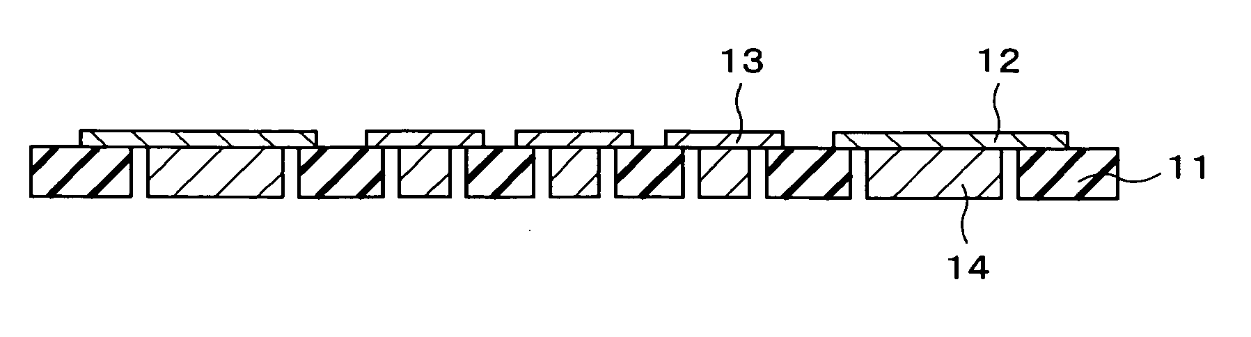
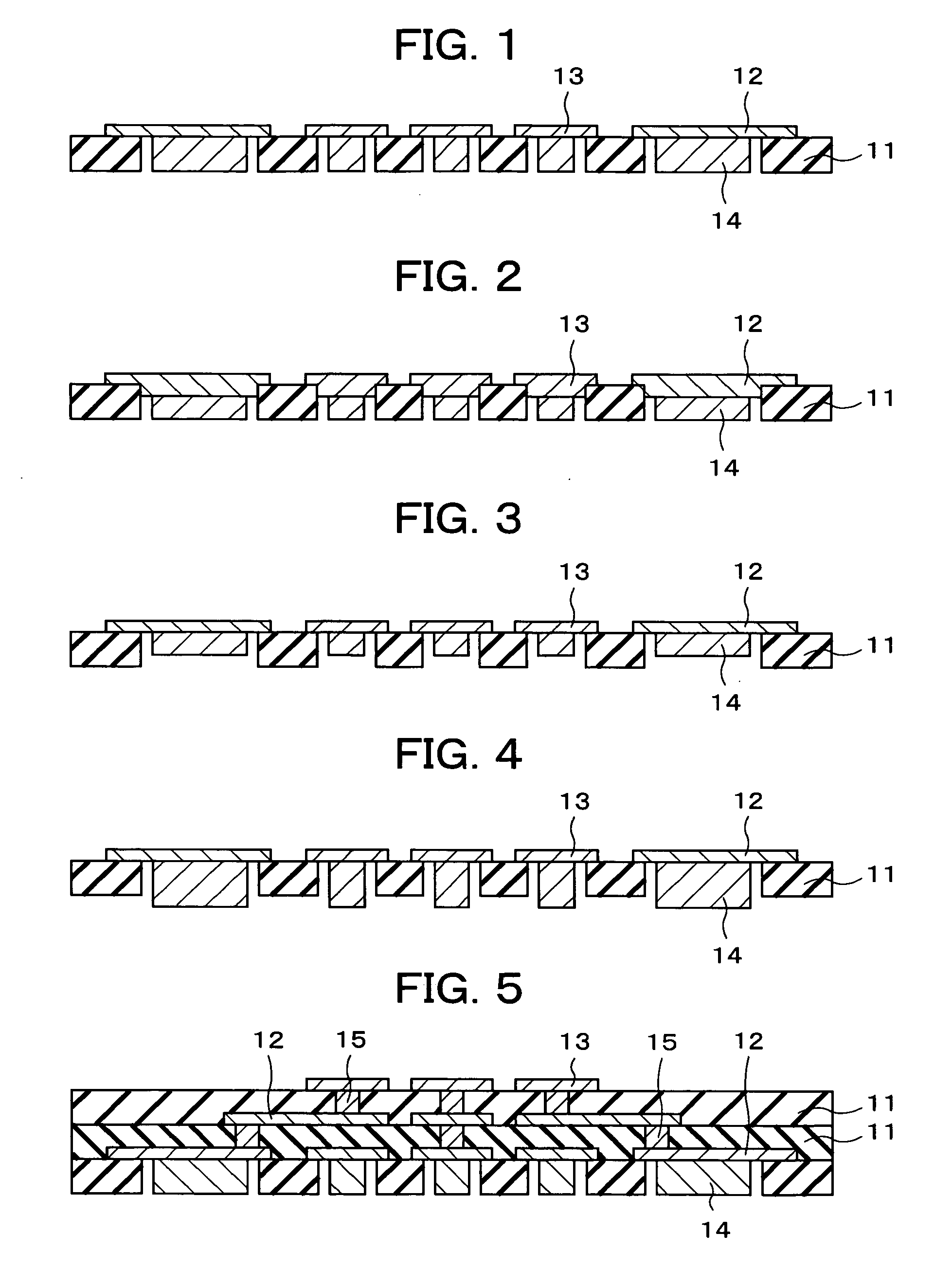
[0099] Embodiments of the present invention are described in detail below with reference to the attached diagrams. Described first is the present invention. FIG. 1 is a schematic cross-sectional view showing an example of a wiring board according to the present embodiment. The wiring substrate shown in FIG. 1 has a structure comprising an insulation layer 11, second electrodes 14 embedded in the insulation layer 11, and a wiring layer 12 and first electrodes 13 disposed on the insulation layer 11 and second electrodes 14, and the side surfaces from among the exposed surfaces of the second electrodes 14 are not in contact with the insulation layer 11.

[0100] The insulation layer 11 is formed, e.g., from a photosensitive or non-photosensitive organic material, and examples of the organic material that may be used include epoxy resin, epoxy acrylate resin, urethane acrylate resin, polyester resin, phenolic resin, polyimide resin, BCB (benzocyclobutene), PBO (polybenzoxazole), polynorbor...

third embodiment

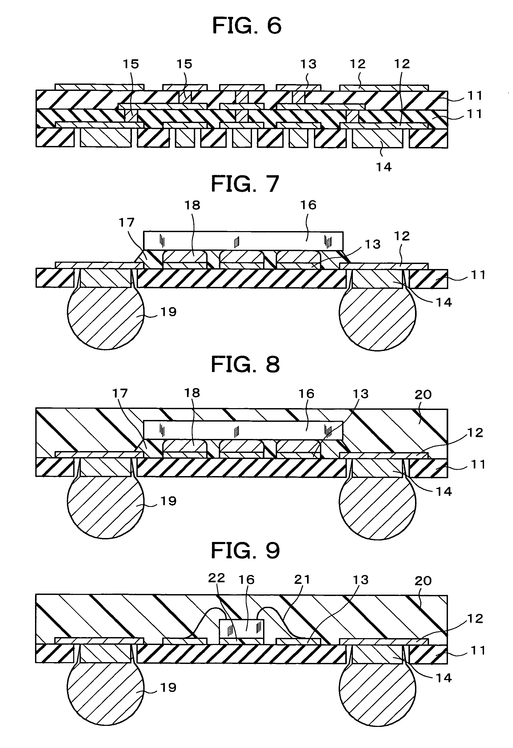
[0134] the present invention is described next. FIG. 7 is a schematic cross-sectional view showing an example of the semiconductor device according to the present embodiment. In FIG. 7, the same reference numerals are used for the same constituent elements as in FIGS. 1 to 6, and a detailed description thereof is omitted. In the semiconductor device according to the present embodiment, a semiconductor element 16 is flip-chip connected by way of solder balls 18 to the first electrodes 13 of the wiring board. The board has a structure comprising an insulation layer 11, second electrodes 14 embedded in the insulation layer 11, and a wiring layer 12 and first electrodes 13 disposed on the insulation layer 11 and second electrodes 14, and the side surfaces from among the exposed surfaces of the second electrodes 14 are not in contact with the insulation layer 11. An underfill resin 17 is filled into the connection portion, and solder balls 19 are disposed on the second electrodes 14, as ...

fourth embodiment

[0157] The effects obtained by the semiconductor device according to the present embodiment are the same as the effects obtained by the semiconductor device described above.

[0158] The sixth embodiment of the present invention is described next. FIG. 10 is a schematic cross-sectional view showing an example of the semiconductor device according to the present embodiment. In FIG. 10, the same reference numerals are used for the same constituent elements as in FIGS. 1 to 9, and a detailed description thereof is omitted. The semiconductor device according to the present embodiment has a structure in which a semiconductor element 24 is mounted on the second electrodes 14, rather than the first electrodes 13 in the semiconductor device according to the third embodiment described above.

[0159] The diagram in FIG. 10 shows an example in which the semiconductor element 24 is mounted on the second electrodes 14 of the wiring board according to the first embodiment of the present invention sh...


PUM


Abstract

A wiring board comprising a first surface on which a first electrode is disposed and a second surface on which a second electrode is disposed; at least a single insulation layer and at least a single wiring layer; and one or a plurality of mounted semiconductor elements, wherein the second electrode disposed on the second surface is embedded in the insulation layer, the surface on the opposite side of the exposed surface on the second surface side of the second electrode is connected to the wiring layer, and all or part of the side surface of the second electrode does not make contact with the insulation layer.

Description

BACKGROUND OF THE INVENTION [0001] 1. Field of the Invention [0002] The present invention relates to a wiring board on which semiconductor elements are mounted, a semiconductor device in which semiconductor elements are mounted on the wiring board, and a method for manufacturing the same, and more specifically relates to a thin wiring board having excellent high-speed transmission characteristics and mounting reliability, and to a semiconductor device in which the wiring board is used. [0003] 2. Description of the Related Art [0004] Electronic devices are rapidly becoming smaller, thinner, and increasingly dense, as recently seen in mobile equipment, and greater thinness, lighter weight, higher density, and other characteristics are needed in wiring boards used in device and semiconductor element mounting due to the increase in the number of terminals associated with higher speeds and functionality of semiconductor elements. [0005] Built-up boards and other boards having through-hol...

Claims


Application Information

Patent Timeline
IPC IPC(8): H01L23/02
CPCH01L21/6835H01L23/49811H01L23/49816H01L23/49838H01L25/0657H01L2221/68345H01L2224/16225H01L2224/48091H01L2224/48227H01L2224/73265H01L2225/0651H01L2225/06517H01L2225/06541H01L2225/06572H01L2225/06586H01L2924/01046H01L2924/01057H01L2924/01078H01L2924/01079H01L2924/09701H01L2924/15311H01L2924/1532H01L2924/19041H01L2924/30107H01L2924/3011H01L2924/3025H05K3/20H05K3/28H05K3/4007H05K2201/0367H05K2201/09881H05K2201/0989H01L2924/00014H01L24/48H01L2924/01019H01L2924/01322H01L2224/32225H01L2224/73204H01L2924/00H01L2924/00012H01L2924/10253H01L2924/181H01L24/73H01L2224/45144H01L24/45H01L2224/45015H01L2924/207
Inventor KIKUCHI, KATSUMIYAMAMICHI, SHINTAROKURITA, YOICHIROSOEJIMA, KOJI
Owner RENESAS ELECTRONICS CORP
Why Eureka
Try Eureka